- 您现在的位置:买卖IC网 > PDF目录225233 > SSQE48T25015-PABN (POWER-ONE INC) 1-OUTPUT 37.5 W DC-DC REG PWR SUPPLY MODULE PDF资料下载
参数资料
| 型号: | SSQE48T25015-PABN |
| 厂商: | POWER-ONE INC |
| 元件分类: | 电源模块 |
| 英文描述: | 1-OUTPUT 37.5 W DC-DC REG PWR SUPPLY MODULE |
| 封装: | ROHS COMPLIANT, SIXTEENTH BRICK PACKAGE-8 |
| 文件页数: | 8/12页 |
| 文件大小: | 449K |
| 代理商: | SSQE48T25015-PABN |
ZD-02084 Rev. 1.2
www.power-one.com
Page 5 of 12
SSQE48T25015 DC-DC Converter Data Sheet
36-75 VDC Input; 1.5 VDC, 25 A Output
Data Sheet
designer must, if necessary, decrease the maximum
current (originally obtained from the derating curves)
by the same percentage to ensure the con
verters
actual output power remains at or below the
maximum allowable output power.
Output Voltage Adjust /TRIM (Pin 6)
The output voltage can be adjusted up 10% or down
20%. The TRIM pin should be left open if trimming is
not being used. To minimize noise pickup, a 0.1 F
capacitor is connected internally between the TRIM
and SENSE(-) pins.
To increase the output voltage, refer to Fig. C. A trim
resistor, RT-INCR, should be connected between the
TRIM (Pin 6) and SENSE(+) (Pin 7), with a value of:
10.22
1.225
Δ
626
Δ)V
5.11(100
R
NOM
O
INCR
T
, [k
],
where,
INCR
T
R
Required value of trim-up resistor [k
]
NOM
O
V
Nominal value of output voltage [V]
100
X
V
)
V
(V
Δ
NOM
-
O
NOM
-
O
REQ
-
O
, [%]
REQ
O
V
Desired (trimmed) output voltage [V].
When trimming up, care must be taken not to exceed
the converters maximum allowable output power.
See the previous section for a complete discussion
of this requirement.
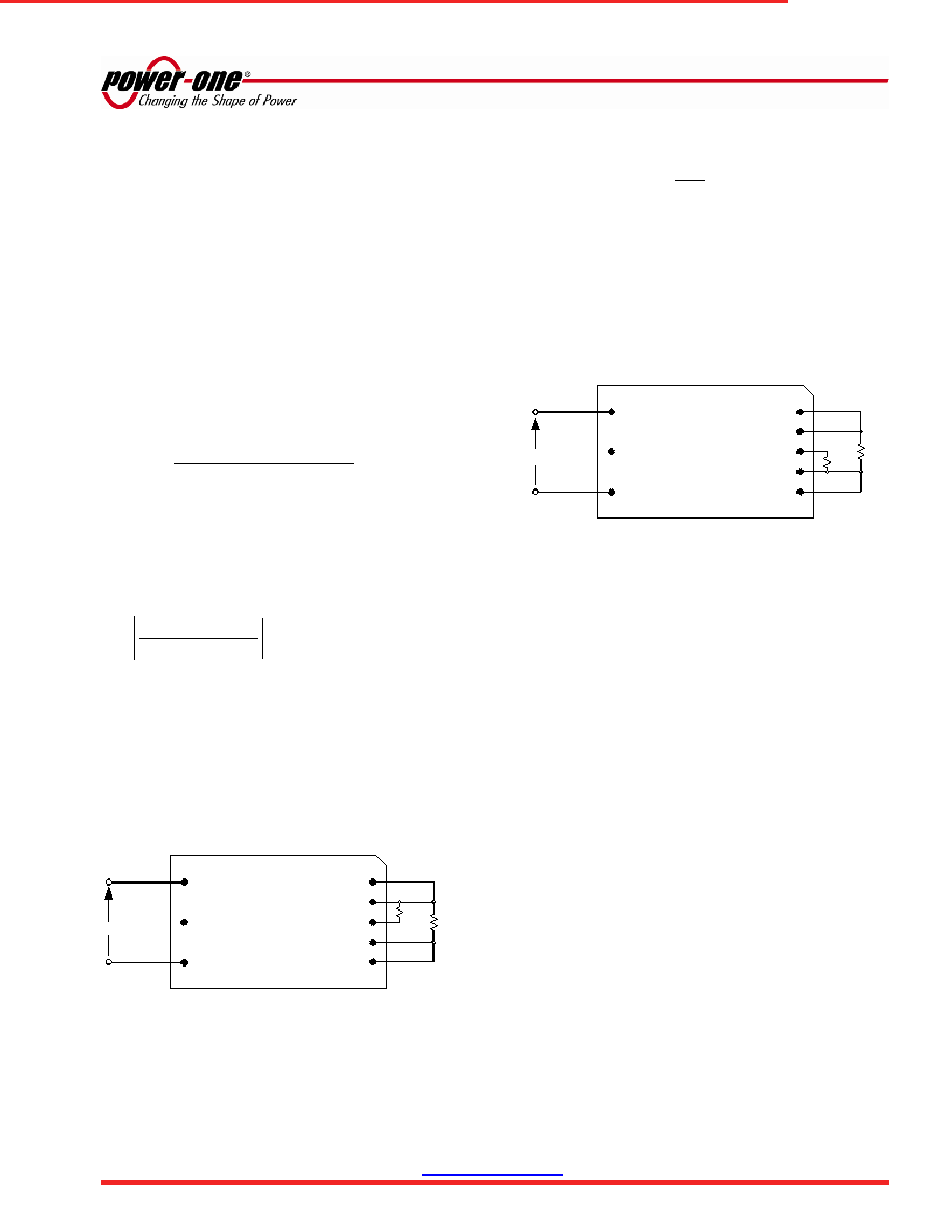
Rload
Vin
Vin (+)
Vin (-)
ON/OFF
Vout (+)
Vout (-)
TRIM
SENSE (+)
SENSE (-)
RT-INCR
(Top View)
SSQE48 Converter
Fig. C: Configuration for increasing output voltage.
To decrease the output voltage (Fig. D), a trim
resistor, RT-DECR, should be connected between the
TRIM (Pin 6) and SENSE(-) (Pin 5), with a value of:
10.22
|
Δ
|
511
R DECR
T
, [k
]
where,
RT-DECR = Required value of trim-down resistor [k]
and
Δ is defined above.
Note:
The above equations for calculation of trim resistor values match
those typically used in conventional industry-standard quarter-
bricks, eighth-bricks and sixteenth-bricks.
Rload
Vin
Vin (+)
Vin (-)
ON/OFF
Vout (+)
Vout (-)
TRIM
SENSE (+)
SENSE (-)
R
T-DECR
(Top View)
SSQE48 Converter
Fig. D: Configuration for decreasing output voltage.
Trimming/sensing beyond 110% of the rated output
voltage is not an acceptable design practice, as this
condition could cause unwanted triggering of the
output overvoltage protection (OVP) circuit. The
designer should ensure that the difference between
the voltages across the converters output pins and
its sense pins does not exceed 10% of VOUT(nom),
or:
X
NOM
-
O
SENSE
OUT
10%
V
)]
(
V
)
(
[V
)]
(
V
)
(
[V
[V]
This equation is applicable for any condition of
output sensing and/or output trim.
相关PDF资料 |
PDF描述 |
|---|---|
| SST-1 | SIP32, IC SOCKET |
| SST270T1 | P-CHANNEL, Si, SMALL SIGNAL, JFET |
| SSTA63T216 | 500 mA, 30 V, PNP, Si, SMALL SIGNAL TRANSISTOR |
| SSTPAD5 | 0.01 A, SILICON, SIGNAL DIODE |
| ST-MS-7-56 | POWER TRANSFORMER, 36 VA |
相关代理商/技术参数 |
参数描述 |
|---|---|
| SSQE48T25015-PABNG | 功能描述:DC/DC转换器 RoHS:否 制造商:Murata 产品: 输出功率: 输入电压范围:3.6 V to 5.5 V 输入电压(标称): 输出端数量:1 输出电压(通道 1):3.3 V 输出电流(通道 1):600 mA 输出电压(通道 2): 输出电流(通道 2): 安装风格:SMD/SMT 封装 / 箱体尺寸: |
| SSQE48T25018-NAANG | 制造商:Power-One 功能描述:Module DC-DC 1-OUT 1.8V 25A 8-Pin 1/16-Brick |
| SSQE48T25018-NAB0G | 制造商:Power-One 功能描述:DCDC - Bulk |
| SSQE48T25018-NABNG | 功能描述:DC/DC转换器 RoHS:否 制造商:Murata 产品: 输出功率: 输入电压范围:3.6 V to 5.5 V 输入电压(标称): 输出端数量:1 输出电压(通道 1):3.3 V 输出电流(通道 1):600 mA 输出电压(通道 2): 输出电流(通道 2): 安装风格:SMD/SMT 封装 / 箱体尺寸: |
| SSQE48T25018-PAA0 | 制造商:Power-One 功能描述:- Bulk |
发布紧急采购,3分钟左右您将得到回复。