- 您现在的位置:买卖IC网 > Datasheet目录885 > SSQE48T25025-PABNG (Power-One)DC/DC SIXTEENTH BRICK Datasheet资料下载
参数资料
| 型号: | SSQE48T25025-PABNG |
| 厂商: | Power-One |
| 文件页数: | 8/12页 |
| 文件大小: | 0K |
| 描述: | DC/DC SIXTEENTH BRICK |
| 标准包装: | 98 |
| 系列: | * |
�� �
�
�SSQE48T25025� DC-DC� Converter�
�36-75� VDC� Input;� 2.5� VDC,� 25� A� Output�
�Data� Sheet�
�Characterization�
�General� Information�
�The� converters� have� been� characterized� for� many�
�operational� aspects,� to� include� thermal� derating�
�(maximum� load� current� as� a� function� of� ambient�
�(ii)� The� temperature� of� the� transformer� does� not�
�exceed� 125� °C,� or�
�(iii)� The� nominal� rating� of� the� converter.�
�During� normal� operation,� derating� curves� with�
�maximum� FET� temperature� less� or� equal� to� 125� °C�
�temperature� and� airflow)� for� vertical� and� horizontal�
�should�
�not� be� exceeded.�
�Temperature�
�at�
�mounting,� efficiency,�
�startup�
�and� shutdown�
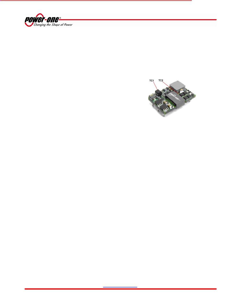
�thermocouple� locations� TC1� and� TC2� shown� in� Fig.� H�
�parameters,� output� ripple� and� noise,� transient�
�response� to� load� step-change,� overload,� and� short�
�circuit.�
�Test� Conditions�
�All� data� presented� were� taken� with� the� converter�
�soldered� to� a� test� board,� specifically� a� 0.060”� thick�
�printed� wiring� board� (PWB)� with� four� layers.� The� top�
�and� bottom� layers� were� not� metallized.� The� two� inner�
�layers,� comprised� of� two-ounce� copper,� were� used� to�
�provide� traces� for� connectivity� to� the� converter.�
�The� lack� of� metallization� on� the� outer� layers� as� well�
�as� the� limited� thermal� connection� ensured� that� heat�
�transfer� from� the� converter� to� the� PWB� was�
�minimized.� This� provides� a� worst-case� but� consistent�
�scenario� for� thermal� derating� purposes.�
�All� measurements� requiring� airflow� were� made� in� the�
�vertical� and� horizontal� wind� tunnel� using� Infrared� (IR)�
�thermography� and� thermocouples� for� thermometry.�
�Ensuring� components� on� the� converter� do� not�
�exceed� their� ratings� is� important� to� maintaining� high�
�reliability.� If� one� anticipates� operating� the� converter�
�at� or� close� to� the� maximum� loads� specified� in� the�
�derating� curves,� it� is� prudent� to� check� actual�
�operating� temperatures� in� the� application.�
�should� not� exceed� 100°C� and� 125°C� respectively,� in�
�order� to� operate� inside� the� derating� curves.�
�Fig.� H:� Locations� of� the� thermocouple� for� thermal� testing.�
�Efficiency�
�Figure� 2� shows� the� efficiency� vs.� load� current� plot� for�
�ambient� temperature� of� 25oC,� airflow� rate� of� 300� LFM�
�(1.5� m/s)� with� vertical� mounting� and� input� voltages� of�
�36V,� 48V,� 54V,� and� 72V.� Also,� a� plot� of� efficiency� vs.�
�load� current,� as� a� function� of� ambient� temperature�
�with� Vin=48V,� airflow� rate� of� 200� LFM� (1� m/s)� with�
�vertical� mounting� is� shown� in� Figure� 3.�
�Power� Dissipation�
�Figure� 4� shows� the� power� dissipation� vs.� load� current�
�plot� for� Ta� =� 25oC,� airflow� rate� of� 300� LFM� (1.5� m/s)�
�Thermographic�
�imaging� is�
�preferable;� if� this�
�with� vertical� mounting� and� input� voltages� of� 36V,� 48V,�
�capability� is� not� available,� then� thermocouples� may�
�be� used.� The� use� of� AWG� #40� gauge� thermocouples�
�is� recommended� to� ensure� measurement� accuracy.�
�Careful� routing� of� the� thermocouple� leads� will� further�
�minimize� measurement� error.� Refer� to� Fig.� H� for� the�
�recommended� measuring� thermocouple� location.�
�Thermal� Derating�
�Load� current� vs.� ambient� temperature� and� airflow�
�54V,� and� 72V.� Also,� a� plot� of� power� dissipation� vs.�
�load� current,� as� a� function� of� ambient� temperature�
�with� Vin=48V,� airflow� rate� of� 200� LFM� (1� m/s)� with�
�vertical� mounting� is� shown� in� Figure� 5.�
�Startup�
�Output� voltage� waveforms� during� the� turn-on� transient�
�using� the� ON/OFF� pin� for� full� rated� load� currents�
�(resistive� load)� are� shown� without� and� with� external�
�rates� are� given� in� Figure� 1.� Ambient� temperature�
�load� capacitance�
�in�
�Figure�
�6�
�and�
�Figure�
�7,�
�was� varied� between� 25� °C� and� 85� °C,� with� airflow�
�rates� from� 30� to� 500� LFM� (0.15� to� 2.5� m/s).�
�For� each� set� of� conditions,� the� maximum� load�
�current� was� defined� as� the� lowest� of:�
�(i)� The� output� current� at� which� any� FET� junction�
�temperature� does� not� exceed� a� maximum� specified�
�temperature� of� 125� °C� as� indicated� by� the�
�thermographic� image,� or�
�respectively.�
�Ripple� and� Noise�
�Figure� 10� shows� the� output� voltage� ripple� waveform,�
�measured� at� full� rated� load� current� with� a� 10� μF�
�tantalum� and� 1� μF� ceramic� capacitor� across� the�
�output.� Note� that� all� output� voltage� waveforms� are�
�measured� across� a� 1� μF� ceramic� capacitor.�
�The� input� reflected-ripple� current� waveforms� are�
�obtained� using� the� test� setup� shown� in� Figure� 11.�
�ZD-02089� Rev.� 1.1�
�www.power-one.com�
�Page� 8� of� 12�
�相关PDF资料 |
PDF描述 |
|---|---|
| SSQL48T20033-NAABG | CONV DC-DC 3.3V 20A 1/16 BRICK |
| ST5ER504 | TRIMMER 500K OHM 0.25W SMD |
| ST7ETB503 | TRIMMER 50K OHM 0.25W SMD |
| SXR471M016ST | CAP ALUM 470UF 16V 20% RADIAL |
| T0053278670 | PUD151R POWER UNIT 230V |
相关代理商/技术参数 |
参数描述 |
|---|---|
| SSQE48T25033-NAAN | 制造商:Power-One 功能描述:SSQE series 3.3 V 25 A Single Output DC/DC Converter |
| SSQE48T25033-NAANG | 功能描述:DC/DC转换器 3.3v 25A NEG TH .188" PL /16TH BRICK RoHS:否 制造商:Murata 产品: 输出功率: 输入电压范围:3.6 V to 5.5 V 输入电压(标称): 输出端数量:1 输出电压(通道 1):3.3 V 输出电流(通道 1):600 mA 输出电压(通道 2): 输出电流(通道 2): 安装风格:SMD/SMT 封装 / 箱体尺寸: |
| SSQE48T25033-NABNG | 功能描述:DC/DC转换器 3.3V 25A NEG TH .145" PL /16TH BRICK RoHS:否 制造商:Murata 产品: 输出功率: 输入电压范围:3.6 V to 5.5 V 输入电压(标称): 输出端数量:1 输出电压(通道 1):3.3 V 输出电流(通道 1):600 mA 输出电压(通道 2): 输出电流(通道 2): 安装风格:SMD/SMT 封装 / 箱体尺寸: |
| SSQE48T25033-PAANG | 功能描述:DC/DC转换器 3.3V 25A POS TH .188" PL /16TH BRICK RoHS:否 制造商:Murata 产品: 输出功率: 输入电压范围:3.6 V to 5.5 V 输入电压(标称): 输出端数量:1 输出电压(通道 1):3.3 V 输出电流(通道 1):600 mA 输出电压(通道 2): 输出电流(通道 2): 安装风格:SMD/SMT 封装 / 箱体尺寸: |
| SSQE48T25033-PABNG | 功能描述:DC/DC转换器 3.3V 25A POS TH .145" PL /16TH BRICK RoHS:否 制造商:Murata 产品: 输出功率: 输入电压范围:3.6 V to 5.5 V 输入电压(标称): 输出端数量:1 输出电压(通道 1):3.3 V 输出电流(通道 1):600 mA 输出电压(通道 2): 输出电流(通道 2): 安装风格:SMD/SMT 封装 / 箱体尺寸: |
发布紧急采购,3分钟左右您将得到回复。