- 您现在的位置:买卖IC网 > PDF目录98144 > ST72121J2T3/XXX (STMICROELECTRONICS) 8-BIT, MROM, 8 MHz, MICROCONTROLLER, PQFP44 PDF资料下载
参数资料
| 型号: | ST72121J2T3/XXX |
| 厂商: | STMICROELECTRONICS |
| 元件分类: | 微控制器/微处理器 |
| 英文描述: | 8-BIT, MROM, 8 MHz, MICROCONTROLLER, PQFP44 |
| 封装: | PLASTIC, TQFP-44 |
| 文件页数: | 58/87页 |
| 文件大小: | 1365K |
| 代理商: | ST72121J2T3/XXX |
第1页第2页第3页第4页第5页第6页第7页第8页第9页第10页第11页第12页第13页第14页第15页第16页第17页第18页第19页第20页第21页第22页第23页第24页第25页第26页第27页第28页第29页第30页第31页第32页第33页第34页第35页第36页第37页第38页第39页第40页第41页第42页第43页第44页第45页第46页第47页第48页第49页第50页第51页第52页第53页第54页第55页第56页第57页当前第58页第59页第60页第61页第62页第63页第64页第65页第66页第67页第68页第69页第70页第71页第72页第73页第74页第75页第76页第77页第78页第79页第80页第81页第82页第83页第84页第85页第86页第87页
61/87
ST72121
SERIAL PERIPHERAL INTERFACE (Cont’d)
4.5.4.3 Data Transfer Format
During an SPI transfer, data is simultaneously
transmitted (shifted out serially) and received
(shifted in serially). The serial clock is used to syn-
chronize the data transfer during a sequence of
eight clock pulses.
The SS pin allows individual selection of a slave
device; the other slave devices that are not select-
ed do not interfere with the SPI transfer.
Clock Phase and Clock Polarity
Four possible timing relationships may be chosen
by software, using the CPOL and CPHA bits.
The CPOL (clock polarity) bit controls the steady
state value of the clock when no data is being
transferred. This bit affects both master and slave
modes.
The combination between the CPOL and CPHA
(clock phase) bits selects the data capture clock
edge.
Figure 37, shows an SPI transfer with the four
combinations of the CPHA and CPOL bits. The di-
agram may be interpreted as a master or slave
timing diagram where the SCK pin, the MISO pin,
the MOSI pin are directly connected between the
master and the slave device.
The SS pin is the slave device select input and can
be driven by the master device.
The master device applies data to its MOSI pin-
clock edge before the capture clock edge.
CPHA bit is set
The second edge on the SCK pin (falling edge if
the CPOL bit is reset, rising edge if the CPOL bit is
set) is the MSBit capture strobe. Data is latched on
the occurrence of the first clock transition.
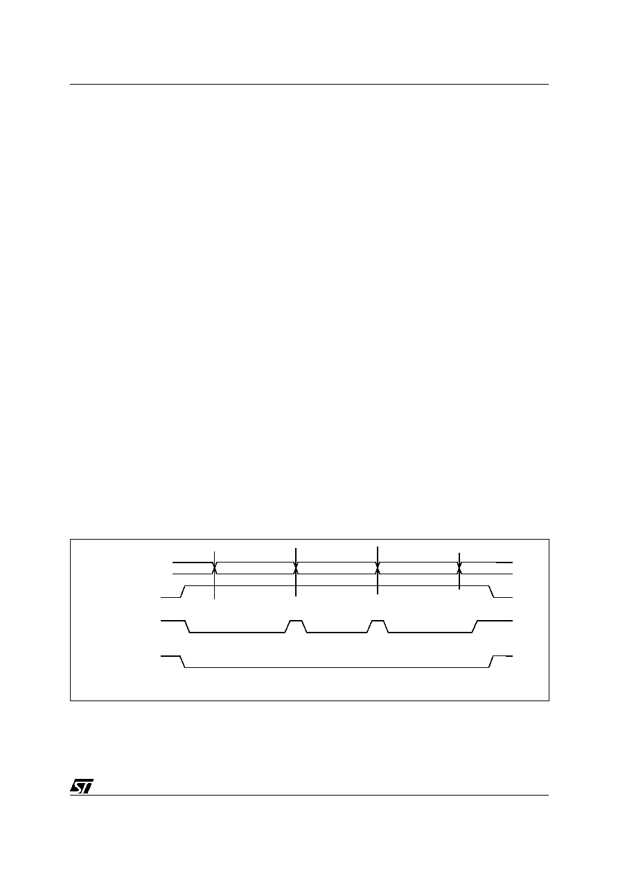
No write collision should occur even if the SS pin
stays low during a transfer of several bytes (see
Figure 36).
CPHA bit is reset
The first edge on the SCK pin (falling edge if CPOL
bitis set,rising edgeifCPOLbit is reset) is the
MSBit capture strobe. Data is latched on the oc-
currence of the second clock transition.
This pin must be toggled high and low between
each byte transmitted (see Figure 36).
To protect the transmission from a write collision a
low value on the SS pin of a slave device freezes
the data in its DR register and does not allow it to
be altered. Therefore the SS pin must be high to
write a new data byte in the DR without producing
a write collision.
Figure 36. CPHA / SS Timing Diagram
MOSI/MISO
Master SS
Slave SS
(CPHA=0)
Slave SS
(CPHA=1)
Byte 1
Byte 2
Byte 3
VR02131C
61
相关PDF资料 |
PDF描述 |
|---|---|
| ST72121J2T6/XXX | 8-BIT, MROM, 16 MHz, MICROCONTROLLER, PQFP44 |
| ST72141K2B3/XXX | 8-BIT, MROM, 8 MHz, MICROCONTROLLER, PDIP32 |
| ST72311N4T6/XXX | 8-BIT, MROM, 8 MHz, MICROCONTROLLER, PQFP64 |
| ST72311J2B6/XXX | 8-BIT, MROM, 8 MHz, MICROCONTROLLER, PDIP42 |
| ST72311N2T3/XXX | 8-BIT, MROM, 8 MHz, MICROCONTROLLER, PQFP64 |
相关代理商/技术参数 |
参数描述 |
|---|---|
| ST72121J4 | 制造商:未知厂家 制造商全称:未知厂家 功能描述:8-BIT MICROCONTROLLER (MCU) WITH 8 TO 16 K ROM/OTP/EPROM. 384 TO 512 BYTES RAM. WDG. SCI. SPI & 2 TIMERS - SDIP42. TQFP44 |
| ST72124J | 制造商:STMICROELECTRONICS 制造商全称:STMicroelectronics 功能描述:8-BIT MCU WITH SINGLE VOLTAGE FLASH MEMORY, ADC, 16-BIT TIMERS, SPI, SCI INTERFACES |
| ST72124J2 | 制造商:STMICROELECTRONICS 制造商全称:STMicroelectronics 功能描述:8-BIT MCU WITH SINGLE VOLTAGE FLASH MEMORY, ADC, 16-BIT TIMERS, SPI, SCI INTERFACES |
| ST72124J2B | 制造商:STMICROELECTRONICS 制造商全称:STMicroelectronics 功能描述:8-BIT MCU WITH SINGLE VOLTAGE FLASH MEMORY, ADC, 16-BIT TIMERS, SPI, SCI INTERFACES |
| ST72124J2B1 | 制造商:STMICROELECTRONICS 制造商全称:STMicroelectronics 功能描述:8-BIT MCU WITH SINGLE VOLTAGE FLASH MEMORY, ADC, 16-BIT TIMERS, SPI, SCI INTERFACES |
发布紧急采购,3分钟左右您将得到回复。