- 您现在的位置:买卖IC网 > PDF目录98144 > ST72311N4T6/XXX (STMICROELECTRONICS) 8-BIT, MROM, 8 MHz, MICROCONTROLLER, PQFP64 PDF资料下载
参数资料
| 型号: | ST72311N4T6/XXX |
| 厂商: | STMICROELECTRONICS |
| 元件分类: | 微控制器/微处理器 |
| 英文描述: | 8-BIT, MROM, 8 MHz, MICROCONTROLLER, PQFP64 |
| 封装: | PLASTIC, TQFP-64 |
| 文件页数: | 9/92页 |
| 文件大小: | 624K |
| 代理商: | ST72311N4T6/XXX |
第1页第2页第3页第4页第5页第6页第7页第8页当前第9页第10页第11页第12页第13页第14页第15页第16页第17页第18页第19页第20页第21页第22页第23页第24页第25页第26页第27页第28页第29页第30页第31页第32页第33页第34页第35页第36页第37页第38页第39页第40页第41页第42页第43页第44页第45页第46页第47页第48页第49页第50页第51页第52页第53页第54页第55页第56页第57页第58页第59页第60页第61页第62页第63页第64页第65页第66页第67页第68页第69页第70页第71页第72页第73页第74页第75页第76页第77页第78页第79页第80页第81页第82页第83页第84页第85页第86页第87页第88页第89页第90页第91页第92页
17/92
ST72311
3.2 RESET
3.2.1 Introduction
There are four sources of Reset:
– RESET pin (external source)
– Power-On Reset (Internal source)
– WATCHDOG (Internal Source)
– Low Voltage Detection Reset (internal source)
The Reset Service Routine vector is located at ad-
dress FFFEh-FFFFh.
3.2.2 External Reset
The RESET pin is both an input and an open-drain
output with integrated pull-up resistor. When one
of the internal Reset sources is active, the Reset
pin is driven low to reset the whole application.
3.2.3 Reset Operation
The duration of the Reset condition, which is also
reflected on the output pin, is fixed at 4096 internal
CPU Clock cycles. A Reset signal originating from
an external source must have a duration of at least
1.5 internal CPU Clock cycles in order to be recog-
nised. At the end of the Power-On Reset cycle, the
MCU may be held in the Reset condition by an Ex-
ternal Reset signal. The RESET pin may thus be
used to ensure VDD has risen to a point where the
MCU can operate correctly before the user pro-
gram is run. Following a Power-On Reset event, or
after exiting Halt mode, a 4096 CPU Clock cycle
delay period is initiated in order to allow the oscil-
lator to stabilise and to ensure that recovery has
taken place from the Reset state.
During the Reset cycle, the device Reset pin acts
as an output that is pulsed low. In its high state, an
internal pull-up resistor is connected to the Reset
pin. This resistor can be pulled low by external cir-
cuitry to reset the device.
The Reset pin is an asynchronous signal which
plays a major role in EMS performance. In a noisy
environment, the best external network is a double
capacitive decoupling consisting of 0.1
Fto V
SS
and 0.1
Fto V
DD.
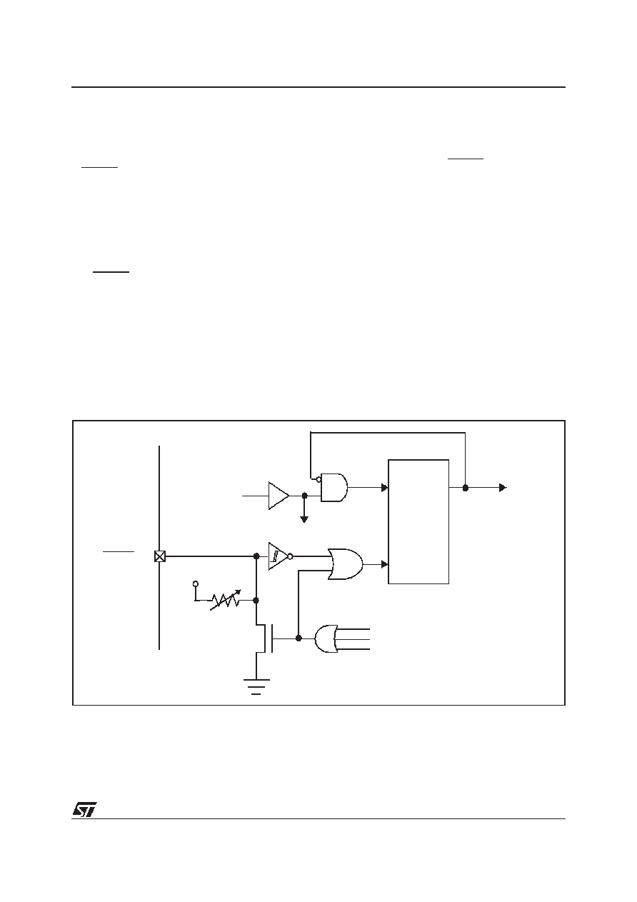
Figure 12. Reset Block Diagram
INTERNAL
RESET
WATCHDOG RESET
OSCILLATOR
SIGNAL
COUNTER
RESET
TO ST7
RESET
POWER-ON RESET
VDD
LOW VOLTAGE DETECTOR RESET
17
相关PDF资料 |
PDF描述 |
|---|---|
| ST72311J2B6/XXX | 8-BIT, MROM, 8 MHz, MICROCONTROLLER, PDIP42 |
| ST72311N2T3/XXX | 8-BIT, MROM, 8 MHz, MICROCONTROLLER, PQFP64 |
| ST72321BAR7T6 | MICROCONTROLLER, QFP64 |
| ST72321BR7T3 | MICROCONTROLLER, QFP64 |
| ST72321M9T3/XXX | 8-BIT, MROM, MICROCONTROLLER, PQFP80 |
相关代理商/技术参数 |
参数描述 |
|---|---|
| ST72311N5B6 | 制造商:未知厂家 制造商全称:未知厂家 功能描述:8-Bit Microcontroller |
| ST72311N6B6 | 制造商:未知厂家 制造商全称:未知厂家 功能描述:8-Bit Microcontroller |
| ST72311R | 制造商:STMICROELECTRONICS 制造商全称:STMicroelectronics 功能描述:8-BIT MCU WITH NESTED INTERRUPTS, EEPROM, ADC, 16-BIT TIMERS, 8-BIT PWM ART, SPI, SCI, CAN INTERFACES |
| ST72311R4Q6 | 制造商:未知厂家 制造商全称:未知厂家 功能描述:8-Bit Microcontroller |
| ST72311R5Q6 | 制造商:未知厂家 制造商全称:未知厂家 功能描述:8-Bit Microcontroller |
发布紧急采购,3分钟左右您将得到回复。