- 您现在的位置:买卖IC网 > PDF目录69366 > ST72621L4T1 (STMICROELECTRONICS) 8-BIT, MROM, 8 MHz, MICROCONTROLLER, PQFP44 PDF资料下载
参数资料
| 型号: | ST72621L4T1 |
| 厂商: | STMICROELECTRONICS |
| 元件分类: | 微控制器/微处理器 |
| 英文描述: | 8-BIT, MROM, 8 MHz, MICROCONTROLLER, PQFP44 |
| 封装: | TQFP-44 |
| 文件页数: | 89/134页 |
| 文件大小: | 815K |
| 代理商: | ST72621L4T1 |
第1页第2页第3页第4页第5页第6页第7页第8页第9页第10页第11页第12页第13页第14页第15页第16页第17页第18页第19页第20页第21页第22页第23页第24页第25页第26页第27页第28页第29页第30页第31页第32页第33页第34页第35页第36页第37页第38页第39页第40页第41页第42页第43页第44页第45页第46页第47页第48页第49页第50页第51页第52页第53页第54页第55页第56页第57页第58页第59页第60页第61页第62页第63页第64页第65页第66页第67页第68页第69页第70页第71页第72页第73页第74页第75页第76页第77页第78页第79页第80页第81页第82页第83页第84页第85页第86页第87页第88页当前第89页第90页第91页第92页第93页第94页第95页第96页第97页第98页第99页第100页第101页第102页第103页第104页第105页第106页第107页第108页第109页第110页第111页第112页第113页第114页第115页第116页第117页第118页第119页第120页第121页第122页第123页第124页第125页第126页第127页第128页第129页第130页第131页第132页第133页第134页
ST7262
58/134
SERIAL PERIPHERAL INTERFACE (Cont’d)
10.4.4.4 Data Transfer Format
During an SPI transfer, data is simultaneously
transmitted (shifted out serially) and received
(shifted in serially). The serial clock is used to syn-
chronize the data transfer during a sequence of
eight clock pulses.
The SS pin allows individual selection of a slave
device; the other slave devices that are not select-
ed do not interfere with the SPI transfer.
Clock Phase and Clock Polarity
Four possible timing relationships may be chosen
by software, using the CPOL and CPHA bits.
The CPOL (clock polarity) bit controls the steady
state value of the clock when no data is being
transferred. This bit affects both master and slave
modes.
The combination between the CPOL and CPHA
(clock phase) bits selects the data capture clock
edge.
Figure 4, shows an SPI transfer with the four com-
binations of the CPHA and CPOL bits. The dia-
gram may be interpreted as a master or slave tim-
ing diagram where the SCK pin, the MISO pin, the
MOSI pin are directly connected between the mas-
ter and the slave device.
The SS pin is the slave device select input and can
be driven by the master device.
The master device applies data to its MOSI pin-
clock edge before the capture clock edge.
CPHA bit is set
The second edge on the SCK pin (falling edge if
the CPOL bit is reset, rising edge if the CPOL bit is
set) is the MSBit capture strobe. Data is latched on
the occurrence of the first clock transition.
No write collision should occur even if the SS pin
stays low during a transfer of several bytes (see
Figure 3).
CPHA bit is reset
The first edge on the SCK pin (falling edge if CPOL
bit is set, rising edge if CPOL bit is reset) is the
MSBit capture strobe. Data is latched on the oc-
currence of the second clock transition.
This pin must be toggled high and low between
each byte transmitted (see Figure 3).
To protect the transmission from a write collision a
low value on the SS pin of a slave device freezes
the data in its SPIDR register and does not allow it
to be altered. Therefore the SS pin must be high to
write a new data byte in the SPIDR without pro-
ducing a write collision.
Note: The SPI must be disabled by resetting the
SPE bit if the CPOL bit is changed at the commu-
nication byte boundaries.
10.4.4.5 Output Disable
In order to free the I/O pin so it can be used for oth-
er purposes, it is possible to disable the SPI output
function by setting the SOD bit in the SPICSR reg-
ister.
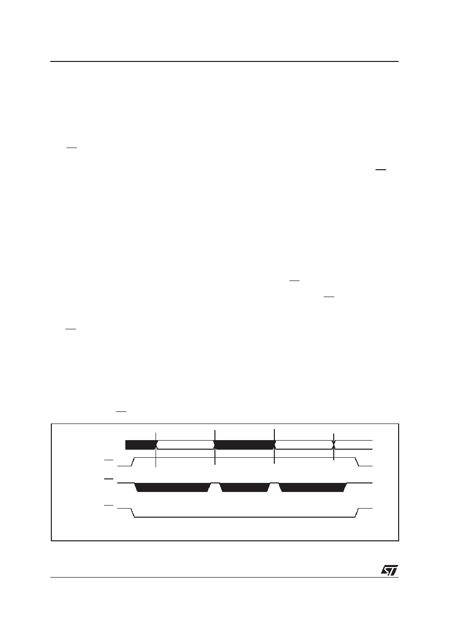
Figure 38. CPHA / SS Timing Diagram
MOSI/MISO
Master SS
Slave SS
(CPHA=0)
Slave SS
(CPHA=1)
Byte 1
Byte 2
Byte 3
1
相关PDF资料 |
PDF描述 |
|---|---|
| ST72632K2B1/XXX | 8-BIT, MROM, 8 MHz, MICROCONTROLLER, PDIP32 |
| ST72E631K4D0 | 8-BIT, UVPROM, 8 MHz, MICROCONTROLLER, PDIP32 |
| ST72633K1M1/XXX | 8-BIT, MROM, 8 MHz, MICROCONTROLLER, PDSO34 |
| ST7263BK1M1/XXX | 8-BIT, MROM, 8 MHz, MICROCONTROLLER, PDSO34 |
| ST72F63BE4M1 | 8-BIT, FLASH, 8 MHz, MICROCONTROLLER, PDSO24 |
相关代理商/技术参数 |
参数描述 |
|---|---|
| ST7263-EMU2 | 功能描述:仿真器/模拟器 ST7 Emulator Board RoHS:否 制造商:Blackhawk 产品:System Trace Emulators 工具用于评估:C6000, C5000, C2000, OMAP, DAVINCI, SITARA, TMS470, TMS570, ARM 7/9, ARM Cortex A8/R4/M3 用于:XDS560v2 |
| ST7265X-EVAL/MS | 制造商:STMicroelectronics 功能描述:ST6 EVAL BD - Bulk |
| ST7265X-EVAL/PFD | 制造商:STMicroelectronics 功能描述:USB FLASH EVAL - Bulk |
| ST7266 | 制造商:6940 功能描述:ST7266 |
| ST7267C8T1L | 制造商:STMicroelectronics 功能描述: |
发布紧急采购,3分钟左右您将得到回复。