- 您现在的位置:买卖IC网 > PDF目录98145 > ST72F321J9T5 (STMICROELECTRONICS) 8-BIT, FLASH, 8 MHz, MICROCONTROLLER, PQFP44 PDF资料下载
参数资料
| 型号: | ST72F321J9T5 |
| 厂商: | STMICROELECTRONICS |
| 元件分类: | 微控制器/微处理器 |
| 英文描述: | 8-BIT, FLASH, 8 MHz, MICROCONTROLLER, PQFP44 |
| 封装: | 10 X 10 MM, PLASTIC, TQFP-44 |
| 文件页数: | 22/176页 |
| 文件大小: | 1112K |
| 代理商: | ST72F321J9T5 |
第1页第2页第3页第4页第5页第6页第7页第8页第9页第10页第11页第12页第13页第14页第15页第16页第17页第18页第19页第20页第21页当前第22页第23页第24页第25页第26页第27页第28页第29页第30页第31页第32页第33页第34页第35页第36页第37页第38页第39页第40页第41页第42页第43页第44页第45页第46页第47页第48页第49页第50页第51页第52页第53页第54页第55页第56页第57页第58页第59页第60页第61页第62页第63页第64页第65页第66页第67页第68页第69页第70页第71页第72页第73页第74页第75页第76页第77页第78页第79页第80页第81页第82页第83页第84页第85页第86页第87页第88页第89页第90页第91页第92页第93页第94页第95页第96页第97页第98页第99页第100页第101页第102页第103页第104页第105页第106页第107页第108页第109页第110页第111页第112页第113页第114页第115页第116页第117页第118页第119页第120页第121页第122页第123页第124页第125页第126页第127页第128页第129页第130页第131页第132页第133页第134页第135页第136页第137页第138页第139页第140页第141页第142页第143页第144页第145页第146页第147页第148页第149页第150页第151页第152页第153页第154页第155页第156页第157页第158页第159页第160页第161页第162页第163页第164页第165页第166页第167页第168页第169页第170页第171页第172页第173页第174页第175页第176页
ST72321J
118/176
I2C BUS INTERFACE (Cont’d)
10.7.7 Register Description
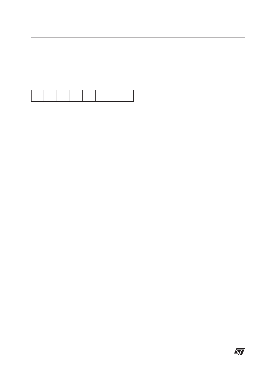
I2C CONTROL REGISTER (CR)
Read / Write
Reset Value: 0000 0000 (00h)
Bit 7:6 = Reserved. Forced to 0 by hardware.
Bit 5 = PE
Peripheral enable.
This bit is set and cleared by software.
0: Peripheral disabled
1: Master/Slave capability
Notes:
– When PE=0, all the bits of the CR register and
the SR register except the Stop bit are reset. All
outputs are released while PE=0
– When PE=1, the corresponding I/O pins are se-
lected by hardware as alternate functions.
– To enable the I
2C interface, write the CR register
TWICE with PE=1 as the first write only activates
the interface (only PE is set).
Bit 4 = ENGC
Enable General Call.
This bit is set and cleared by software. It is also
cleared by hardware when the interface is disa-
bled (PE=0). The 00h General Call address is ac-
knowledged (01h ignored).
0: General Call disabled
1: General Call enabled
Bit 3 = START
Generation of a Start condition.
This bit is set and cleared by software. It is also
cleared by hardware when the interface is disa-
bled (PE=0) or when the Start condition is sent
(with interrupt generation if ITE=1).
– In master mode:
0: No start generation
1: Repeated start generation
– In slave mode:
0: No start generation
1: Start generation when the bus is free
Bit 2 = ACK
Acknowledge enable.
This bit is set and cleared by software. It is also
cleared by hardware when the interface is disa-
bled (PE=0).
0: No acknowledge returned
1: Acknowledge returned after an address byte or
a data byte is received
Bit 1 = STOP
Generation of a Stop condition.
This bit is set and cleared by software. It is also
cleared by hardware in master mode. Note: This
bit is not cleared when the interface is disabled
(PE=0).
– In master mode:
0: No stop generation
1: Stop generation after the current byte transfer
or after the current Start condition is sent. The
STOP bit is cleared by hardware when the Stop
condition is sent.
– In slave mode:
0: No stop generation
1: Release the SCL and SDA lines after the cur-
rent byte transfer (BTF=1). In this mode the
STOP bit has to be cleared by software.
Bit 0 = ITE
Interrupt enable.
This bit is set and cleared by software and cleared
by hardware when the interface is disabled
(PE=0).
0: Interrupts disabled
1: Interrupts enabled
Refer to Figure 64 for the relationship between the
events and the interrupt.
SCL is held low when the ADD10, SB, BTF or
ADSL flags or an EV6 event (See Figure 63) is de-
tected.
70
0
PE
ENGC STA RT
ACK
STOP
ITE
相关PDF资料 |
PDF描述 |
|---|---|
| ST72F324BJ6B6 | 8-BIT, FLASH, 8 MHz, MICROCONTROLLER, PDIP42 |
| ST72F324BK6T6 | 8-BIT, FLASH, 8 MHz, MICROCONTROLLER, PQFP32 |
| ST72F324BK4T6 | 8-BIT, FLASH, 8 MHz, MICROCONTROLLER, PQFP32 |
| ST72F324BJ4B5 | 8-BIT, FLASH, 8 MHz, MICROCONTROLLER, PDIP42 |
| ST72F324BJ2B5 | 8-BIT, FLASH, 8 MHz, MICROCONTROLLER, PDIP42 |
相关代理商/技术参数 |
参数描述 |
|---|---|
| ST72F321J9T6 | 功能描述:8位微控制器 -MCU Flash 60K SPI/SCI/I2 RoHS:否 制造商:Silicon Labs 核心:8051 处理器系列:C8051F39x 数据总线宽度:8 bit 最大时钟频率:50 MHz 程序存储器大小:16 KB 数据 RAM 大小:1 KB 片上 ADC:Yes 工作电源电压:1.8 V to 3.6 V 工作温度范围:- 40 C to + 105 C 封装 / 箱体:QFN-20 安装风格:SMD/SMT |
| ST72F321J9TA | 功能描述:8位微控制器 -MCU AUTO 8BIT MICRO RoHS:否 制造商:Silicon Labs 核心:8051 处理器系列:C8051F39x 数据总线宽度:8 bit 最大时钟频率:50 MHz 程序存储器大小:16 KB 数据 RAM 大小:1 KB 片上 ADC:Yes 工作电源电压:1.8 V to 3.6 V 工作温度范围:- 40 C to + 105 C 封装 / 箱体:QFN-20 安装风格:SMD/SMT |
| ST72F321J9TAE | 功能描述:8位微控制器 -MCU 8B MCU RoHS:否 制造商:Silicon Labs 核心:8051 处理器系列:C8051F39x 数据总线宽度:8 bit 最大时钟频率:50 MHz 程序存储器大小:16 KB 数据 RAM 大小:1 KB 片上 ADC:Yes 工作电源电压:1.8 V to 3.6 V 工作温度范围:- 40 C to + 105 C 封装 / 箱体:QFN-20 安装风格:SMD/SMT |
| ST72F321J9TAS | 制造商:STMicroelectronics 功能描述: |
| ST72F321J9TC | 功能描述:8位微控制器 -MCU Flask 60K SPI/SCI/I2 RoHS:否 制造商:Silicon Labs 核心:8051 处理器系列:C8051F39x 数据总线宽度:8 bit 最大时钟频率:50 MHz 程序存储器大小:16 KB 数据 RAM 大小:1 KB 片上 ADC:Yes 工作电源电压:1.8 V to 3.6 V 工作温度范围:- 40 C to + 105 C 封装 / 箱体:QFN-20 安装风格:SMD/SMT |
发布紧急采购,3分钟左右您将得到回复。