- 您现在的位置:买卖IC网 > PDF目录69364 > ST72F561AR4TAS (STMICROELECTRONICS) 8-BIT, FLASH, 8 MHz, MICROCONTROLLER, PQFP64 PDF资料下载
参数资料
| 型号: | ST72F561AR4TAS |
| 厂商: | STMICROELECTRONICS |
| 元件分类: | 微控制器/微处理器 |
| 英文描述: | 8-BIT, FLASH, 8 MHz, MICROCONTROLLER, PQFP64 |
| 封装: | 10 X 10 MM, ROHS COMPLIANT, LQFP-64 |
| 文件页数: | 199/280页 |
| 文件大小: | 2307K |
| 代理商: | ST72F561AR4TAS |
第1页第2页第3页第4页第5页第6页第7页第8页第9页第10页第11页第12页第13页第14页第15页第16页第17页第18页第19页第20页第21页第22页第23页第24页第25页第26页第27页第28页第29页第30页第31页第32页第33页第34页第35页第36页第37页第38页第39页第40页第41页第42页第43页第44页第45页第46页第47页第48页第49页第50页第51页第52页第53页第54页第55页第56页第57页第58页第59页第60页第61页第62页第63页第64页第65页第66页第67页第68页第69页第70页第71页第72页第73页第74页第75页第76页第77页第78页第79页第80页第81页第82页第83页第84页第85页第86页第87页第88页第89页第90页第91页第92页第93页第94页第95页第96页第97页第98页第99页第100页第101页第102页第103页第104页第105页第106页第107页第108页第109页第110页第111页第112页第113页第114页第115页第116页第117页第118页第119页第120页第121页第122页第123页第124页第125页第126页第127页第128页第129页第130页第131页第132页第133页第134页第135页第136页第137页第138页第139页第140页第141页第142页第143页第144页第145页第146页第147页第148页第149页第150页第151页第152页第153页第154页第155页第156页第157页第158页第159页第160页第161页第162页第163页第164页第165页第166页第167页第168页第169页第170页第171页第172页第173页第174页第175页第176页第177页第178页第179页第180页第181页第182页第183页第184页第185页第186页第187页第188页第189页第190页第191页第192页第193页第194页第195页第196页第197页第198页当前第199页第200页第201页第202页第203页第204页第205页第206页第207页第208页第209页第210页第211页第212页第213页第214页第215页第216页第217页第218页第219页第220页第221页第222页第223页第224页第225页第226页第227页第228页第229页第230页第231页第232页第233页第234页第235页第236页第237页第238页第239页第240页第241页第242页第243页第244页第245页第246页第247页第248页第249页第250页第251页第252页第253页第254页第255页第256页第257页第258页第259页第260页第261页第262页第263页第264页第265页第266页第267页第268页第269页第270页第271页第272页第273页第274页第275页第276页第277页第278页第279页第280页
Revision history
ST72561-Auto
278/280
Doc ID 12370 Rev 7
24
Revision history
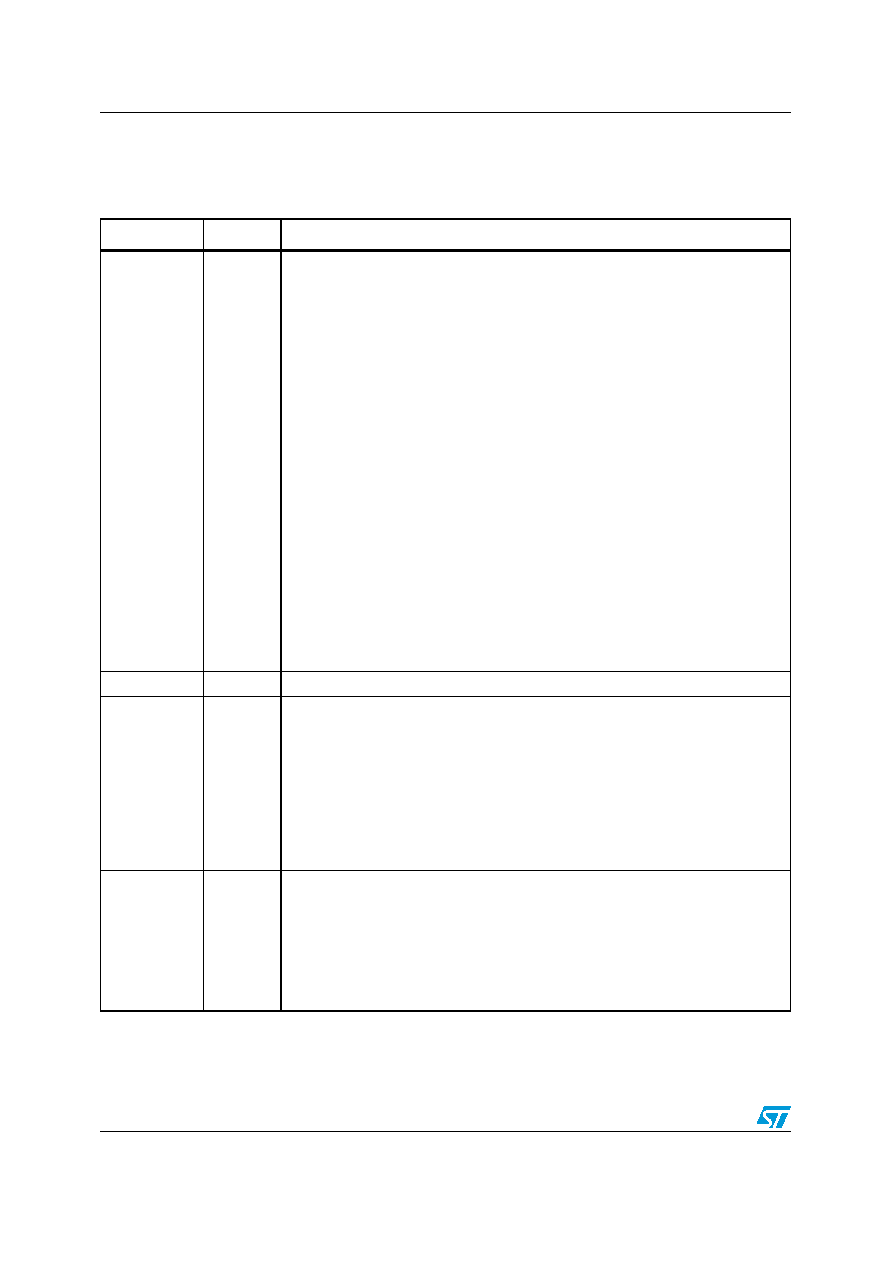
Table 120.
Document revision history
Date
Revision
Changes
03-May-2004
1
Added TQFP 10x10 package
Removed internal RC
Updated Figure 11: Clock, reset and supply block diagram
Added note on monotonous VDD ramp on Section 5.6.1: Low voltage detector (LVD)
Added caution ART Ext clock not available in HALT see Section 11: PWM auto-
reload timer (ART)
Added note “Once the OCIE bit is set both output compare features may trigger...”
and “Once the ICIE bit is set both input capture features may trigger...” in 8-bit timer
Section 13: 8-bit timer (TIM8).
Changed clock from fcpu/8000 to fosc2/8000 in Section 13: 8-bit timer (TIM8)
Changed description of CSR register to read only except bit 2 R/W Section 13: 8-bit
timer (TIM8)
Added note to SPI slave freq. and updated Master mode procedure in Section 14:
Serial peripheral interface (SPI)
Changed description of NF bit in Section 15.10: LIN mode register description
Removed “Configurable timer resolution” under "Time triggered communication
option" from Section 17: beCAN controller (beCAN)
Added Clearing interrupts limitation and SCI wrong break duration to Chapter 24:
Important notes
Removed beCAN Time triggered mode feature from Section 17: beCAN controller
(beCAN)
Renamed CMSR RX and TX bits to REC and TRAN in Section 17: beCAN controller
(beCAN)
Added beCAN FIFO corruption limitation FIFO corruption
Modified IINJ for Port B3 in Section 20.9.1: General characteristics
11-May-2004
2
Modified Clearing interrupts limitation in Chapter 24: Important notes
12-May-2005
3
LIN
SCITM changed to LINSCITM throughout document.
Changed name of WWDGR register to WDGWR in Table 4: Hardware register map
Changed Static power consumption to 200 uA typ in Section 20.9.1: General
characteristics
Modified Readout Protection description in Section 3.3.1: Read-out protection
Added Section 24.1: All devices
Modified Figure 135: RESET pin protection when LVD is enabled and Figure 136:
RESET pin protection when LVD is disabled and related notes
Added 48K ROM version in Table 2: Product overview, Figure 5: Memory map and
Figure 154: ST72561xxx-Auto ROM commercial product structure
24-Oct-2005
4
Added standard version 16K ROM/Flash devices
Modified data retention in Section 20.7: Memory characteristics
Added “6” and “3” standard version device type coding to Figure 152: ST72F561xxx-
Auto Flash commercial product structure and Figure 154: ST72561xxx-Auto ROM
commercial product structure
Modified power consumption Section 20.4: Supply current characteristics
Added CDM in Electrostatic discharge (ESD)
Added “External interrupt missed” Section 24.1.3: External interrupt missed
相关PDF资料 |
PDF描述 |
|---|---|
| ST72561AR4TC/XXXRS | 8-BIT, MROM, 8 MHz, MICROCONTROLLER, PQFP64 |
| ST72561AR4TC/XXXXS | 8-BIT, MROM, 8 MHz, MICROCONTROLLER, PQFP64 |
| ST72561AR6TA/XXXS | 8-BIT, MROM, 8 MHz, MICROCONTROLLER, PQFP64 |
| ST72561AR6TC/XXXRE | 8-BIT, MROM, 8 MHz, MICROCONTROLLER, PQFP64 |
| ST72561AR6TC/XXXRS | 8-BIT, MROM, 8 MHz, MICROCONTROLLER, PQFP64 |
相关代理商/技术参数 |
参数描述 |
|---|---|
| ST72F561AR4TATRE | 制造商:STMicroelectronics 功能描述: |
| ST72F561AR4TCE | 制造商:STMicroelectronics 功能描述: |
| ST72F561AR4TCTRE | 制造商:STMicroelectronics 功能描述: |
| ST72F561AR6T3 | 功能描述:8位微控制器 -MCU ST72561 8B MCU RoHS:否 制造商:Silicon Labs 核心:8051 处理器系列:C8051F39x 数据总线宽度:8 bit 最大时钟频率:50 MHz 程序存储器大小:16 KB 数据 RAM 大小:1 KB 片上 ADC:Yes 工作电源电压:1.8 V to 3.6 V 工作温度范围:- 40 C to + 105 C 封装 / 箱体:QFN-20 安装风格:SMD/SMT |
| ST72F561AR6TAE | 功能描述:8位微控制器 -MCU 8B MCU RoHS:否 制造商:Silicon Labs 核心:8051 处理器系列:C8051F39x 数据总线宽度:8 bit 最大时钟频率:50 MHz 程序存储器大小:16 KB 数据 RAM 大小:1 KB 片上 ADC:Yes 工作电源电压:1.8 V to 3.6 V 工作温度范围:- 40 C to + 105 C 封装 / 箱体:QFN-20 安装风格:SMD/SMT |
发布紧急采购,3分钟左右您将得到回复。