- 您现在的位置:买卖IC网 > PDF目录69380 > ST92F120JV1Q (STMICROELECTRONICS) 16-BIT, FLASH, 24 MHz, MICROCONTROLLER, PQFP100 PDF资料下载
参数资料
| 型号: | ST92F120JV1Q |
| 厂商: | STMICROELECTRONICS |
| 元件分类: | 微控制器/微处理器 |
| 英文描述: | 16-BIT, FLASH, 24 MHz, MICROCONTROLLER, PQFP100 |
| 封装: | PLASTIC, QFP-100 |
| 文件页数: | 213/320页 |
| 文件大小: | 1895K |
| 代理商: | ST92F120JV1Q |
第1页第2页第3页第4页第5页第6页第7页第8页第9页第10页第11页第12页第13页第14页第15页第16页第17页第18页第19页第20页第21页第22页第23页第24页第25页第26页第27页第28页第29页第30页第31页第32页第33页第34页第35页第36页第37页第38页第39页第40页第41页第42页第43页第44页第45页第46页第47页第48页第49页第50页第51页第52页第53页第54页第55页第56页第57页第58页第59页第60页第61页第62页第63页第64页第65页第66页第67页第68页第69页第70页第71页第72页第73页第74页第75页第76页第77页第78页第79页第80页第81页第82页第83页第84页第85页第86页第87页第88页第89页第90页第91页第92页第93页第94页第95页第96页第97页第98页第99页第100页第101页第102页第103页第104页第105页第106页第107页第108页第109页第110页第111页第112页第113页第114页第115页第116页第117页第118页第119页第120页第121页第122页第123页第124页第125页第126页第127页第128页第129页第130页第131页第132页第133页第134页第135页第136页第137页第138页第139页第140页第141页第142页第143页第144页第145页第146页第147页第148页第149页第150页第151页第152页第153页第154页第155页第156页第157页第158页第159页第160页第161页第162页第163页第164页第165页第166页第167页第168页第169页第170页第171页第172页第173页第174页第175页第176页第177页第178页第179页第180页第181页第182页第183页第184页第185页第186页第187页第188页第189页第190页第191页第192页第193页第194页第195页第196页第197页第198页第199页第200页第201页第202页第203页第204页第205页第206页第207页第208页第209页第210页第211页第212页当前第213页第214页第215页第216页第217页第218页第219页第220页第221页第222页第223页第224页第225页第226页第227页第228页第229页第230页第231页第232页第233页第234页第235页第236页第237页第238页第239页第240页第241页第242页第243页第244页第245页第246页第247页第248页第249页第250页第251页第252页第253页第254页第255页第256页第257页第258页第259页第260页第261页第262页第263页第264页第265页第266页第267页第268页第269页第270页第271页第272页第273页第274页第275页第276页第277页第278页第279页第280页第281页第282页第283页第284页第285页第286页第287页第288页第289页第290页第291页第292页第293页第294页第295页第296页第297页第298页第299页第300页第301页第302页第303页第304页第305页第306页第307页第308页第309页第310页第311页第312页第313页第314页第315页第316页第317页第318页第319页第320页
290/320
EIGHT-CHANNEL ANALOG TO DIGITAL CONVERTER (A/D)
ANALOG TO DIGITAL CONVERTER (Cont’d)
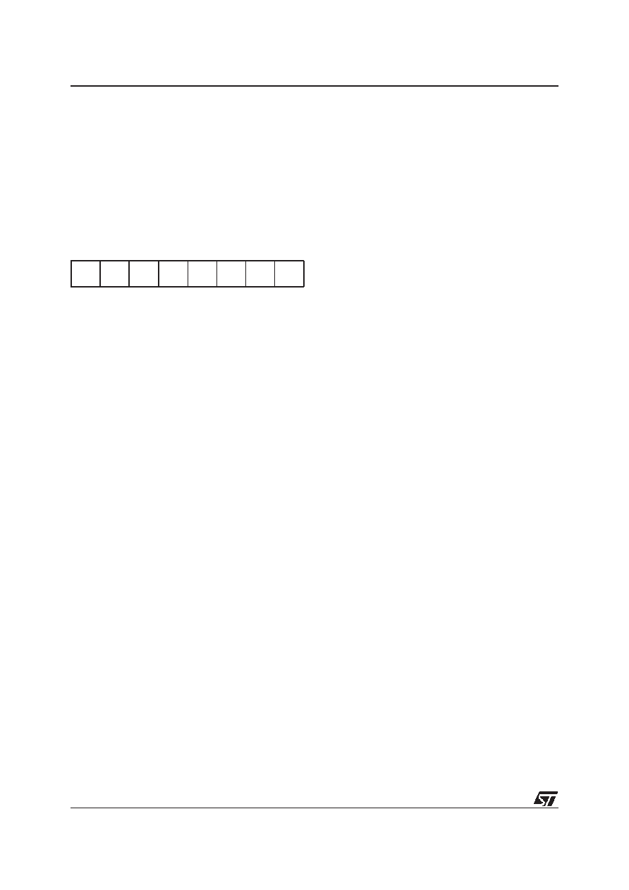
CONTROL LOGIC REGISTER (CLR)
The Control Logic Register (CLR) manages the
A/D converter logic. Writing to this register will
cause the current conversion to be aborted and
the autoscan logic to be re-initialized.
CONTROL LOGIC REGISTER (CLR)
R253 - Read/Write
Register Page: 63
Reset Value: 0000 0000 (00h)
Bit 7:5 = SC[2:0]:
Start Conversion Address.
These 3 bits define the starting analog input chan-
nel (Autoscan mode). The first channel addressed
by SC[2:0] is converted, then the channel number
is incremented for the successive conversion, until
channel 7 (111) is converted. When SC2, SC1 and
SC0 are all set, only channel 7 will be converted.
Bit 4 = EXTG:
External Trigger Enable.
This bit is set and cleared by software.
0: External trigger disabled.
1: External trigger enabled. Allows a conversion
sequence to be started on the subsequent edge
of the external signal applied to the EXTRG pin
(when enabled as an Alternate Function).
Bit 3 = INTG:
Internal Trigger Enable.
This bit is set and cleared by software.
0: Internal trigger disabled.
1: Internal trigger enabled. Allows a conversion se-
quence to be started, synchronized by an inter-
nal signal (On-chip Event signal) from a Multi-
function Timer peripheral.
Both External and Internal Trigger inputs are inter-
nally ORed, thus avoiding Hardware conflicts;
however, the correct procedure is to enable only
one alternate synchronization input at a time.
Note: The effect of either synchronization mode is
to set the START/STOP bit, which is reset by hard-
ware when in SINGLE mode, at the end of each
sequence of conversions.
Requirements: The External Synchronisation In-
put must receive a low level pulse longer than an
INTCLK period and, for both External and On-Chip
Event synchronisation, the repetition period must
be greater than the time required for the selected
sequence of conversions.
Bit 2 = POW:
Power Up/Power Down.
This bit is set and cleared by software.
0: Power down mode: all power-consuming logic is
disabled, thus selecting a low power idle mode.
1: Power up mode: the A/D converter logic and an-
alog circuitry is enabled.
Bit 1 = CONT:
Continuous/Single.
0: Single Mode: a single sequence of conversions
is initiated whenever an external (or internal)
trigger occurs, or when the ST bit is set by soft-
ware.
1: Continuous Mode: the first sequence of conver-
sions is started, either by software (by setting
the ST bit), or by hardware (on an internal or ex-
ternal trigger, depending on the setting of the
INTG and EXTG bits); a continuous conversion
sequence is then initiated.
Bit 0 = ST:
Start/Stop.
0: Stop conversion. When the A/D converter is
running in Single Mode, this bit is hardware re-
set at the end of a sequence of conversions.
1: Start a sequence of conversions.
70
SC2
SC1
SC0
EXT
G
INTG POW
CON
T
ST
9
相关PDF资料 |
PDF描述 |
|---|---|
| ST92F120R1Q6 | 16-BIT, FLASH, 24 MHz, MICROCONTROLLER, PQFP64 |
| ST92F120JR1Q7 | 16-BIT, FLASH, 24 MHz, MICROCONTROLLER, PQFP64 |
| ST92F150CV1Q6 | 16-BIT, FLASH, 24 MHz, MICROCONTROLLER, PQFP100 |
| ST92F150JDV1T6 | 16-BIT, FLASH, 24 MHz, MICROCONTROLLER, PQFP100 |
| ST92F150CV1T6 | 16-BIT, FLASH, 24 MHz, MICROCONTROLLER, PQFP100 |
相关代理商/技术参数 |
参数描述 |
|---|---|
| ST92F120V1Q7 | 功能描述:8位微控制器 -MCU Flash 128K SPI/I2C RoHS:否 制造商:Silicon Labs 核心:8051 处理器系列:C8051F39x 数据总线宽度:8 bit 最大时钟频率:50 MHz 程序存储器大小:16 KB 数据 RAM 大小:1 KB 片上 ADC:Yes 工作电源电压:1.8 V to 3.6 V 工作温度范围:- 40 C to + 105 C 封装 / 箱体:QFN-20 安装风格:SMD/SMT |
| ST92F120V9Q7 | 功能描述:8位微控制器 -MCU RO 511-ST92F150CV1QB RoHS:否 制造商:Silicon Labs 核心:8051 处理器系列:C8051F39x 数据总线宽度:8 bit 最大时钟频率:50 MHz 程序存储器大小:16 KB 数据 RAM 大小:1 KB 片上 ADC:Yes 工作电源电压:1.8 V to 3.6 V 工作温度范围:- 40 C to + 105 C 封装 / 箱体:QFN-20 安装风格:SMD/SMT |
| ST92F124R9TB | 功能描述:8位微控制器 -MCU Flash 64K SCI/SPI/I2 RoHS:否 制造商:Silicon Labs 核心:8051 处理器系列:C8051F39x 数据总线宽度:8 bit 最大时钟频率:50 MHz 程序存储器大小:16 KB 数据 RAM 大小:1 KB 片上 ADC:Yes 工作电源电压:1.8 V to 3.6 V 工作温度范围:- 40 C to + 105 C 封装 / 箱体:QFN-20 安装风格:SMD/SMT |
| ST92F124V1QB | 功能描述:8位微控制器 -MCU Flash 128K 2SCI/SPI RoHS:否 制造商:Silicon Labs 核心:8051 处理器系列:C8051F39x 数据总线宽度:8 bit 最大时钟频率:50 MHz 程序存储器大小:16 KB 数据 RAM 大小:1 KB 片上 ADC:Yes 工作电源电压:1.8 V to 3.6 V 工作温度范围:- 40 C to + 105 C 封装 / 箱体:QFN-20 安装风格:SMD/SMT |
| ST92F124V1T6 | 功能描述:8位微控制器 -MCU 8/16-BIT SINGLE VOLT RoHS:否 制造商:Silicon Labs 核心:8051 处理器系列:C8051F39x 数据总线宽度:8 bit 最大时钟频率:50 MHz 程序存储器大小:16 KB 数据 RAM 大小:1 KB 片上 ADC:Yes 工作电源电压:1.8 V to 3.6 V 工作温度范围:- 40 C to + 105 C 封装 / 箱体:QFN-20 安装风格:SMD/SMT |
发布紧急采购,3分钟左右您将得到回复。