- 您现在的位置:买卖IC网 > PDF目录69380 > ST92F120JV1Q (STMICROELECTRONICS) 16-BIT, FLASH, 24 MHz, MICROCONTROLLER, PQFP100 PDF资料下载
参数资料
| 型号: | ST92F120JV1Q |
| 厂商: | STMICROELECTRONICS |
| 元件分类: | 微控制器/微处理器 |
| 英文描述: | 16-BIT, FLASH, 24 MHz, MICROCONTROLLER, PQFP100 |
| 封装: | PLASTIC, QFP-100 |
| 文件页数: | 44/320页 |
| 文件大小: | 1895K |
| 代理商: | ST92F120JV1Q |
第1页第2页第3页第4页第5页第6页第7页第8页第9页第10页第11页第12页第13页第14页第15页第16页第17页第18页第19页第20页第21页第22页第23页第24页第25页第26页第27页第28页第29页第30页第31页第32页第33页第34页第35页第36页第37页第38页第39页第40页第41页第42页第43页当前第44页第45页第46页第47页第48页第49页第50页第51页第52页第53页第54页第55页第56页第57页第58页第59页第60页第61页第62页第63页第64页第65页第66页第67页第68页第69页第70页第71页第72页第73页第74页第75页第76页第77页第78页第79页第80页第81页第82页第83页第84页第85页第86页第87页第88页第89页第90页第91页第92页第93页第94页第95页第96页第97页第98页第99页第100页第101页第102页第103页第104页第105页第106页第107页第108页第109页第110页第111页第112页第113页第114页第115页第116页第117页第118页第119页第120页第121页第122页第123页第124页第125页第126页第127页第128页第129页第130页第131页第132页第133页第134页第135页第136页第137页第138页第139页第140页第141页第142页第143页第144页第145页第146页第147页第148页第149页第150页第151页第152页第153页第154页第155页第156页第157页第158页第159页第160页第161页第162页第163页第164页第165页第166页第167页第168页第169页第170页第171页第172页第173页第174页第175页第176页第177页第178页第179页第180页第181页第182页第183页第184页第185页第186页第187页第188页第189页第190页第191页第192页第193页第194页第195页第196页第197页第198页第199页第200页第201页第202页第203页第204页第205页第206页第207页第208页第209页第210页第211页第212页第213页第214页第215页第216页第217页第218页第219页第220页第221页第222页第223页第224页第225页第226页第227页第228页第229页第230页第231页第232页第233页第234页第235页第236页第237页第238页第239页第240页第241页第242页第243页第244页第245页第246页第247页第248页第249页第250页第251页第252页第253页第254页第255页第256页第257页第258页第259页第260页第261页第262页第263页第264页第265页第266页第267页第268页第269页第270页第271页第272页第273页第274页第275页第276页第277页第278页第279页第280页第281页第282页第283页第284页第285页第286页第287页第288页第289页第290页第291页第292页第293页第294页第295页第296页第297页第298页第299页第300页第301页第302页第303页第304页第305页第306页第307页第308页第309页第310页第311页第312页第313页第314页第315页第316页第317页第318页第319页第320页
138/320
STANDARD TIMER (STIM)
STANDARD TIMER (Cont’d)
10.2.2.4 Standard Timer Output Modes
OUTPUT modes are selected using 2 bits of the
STC register: OUTMD1 and OUTMD2.
No Output Mode (OUTMD1 = “0”, OUTMD2 = “0”)
The output is disabled and the corresponding pin
is set high, in order to allow other alternate func-
tions to use the I/O pin.
Square Wave Output Mode (OUTMD1 = “0”,
OUTMD2 = “1”)
The Standard Timer toggles the state of the
STOUT pin on every End Of Count condition. With
INTCLK = 12MHz, this allows generation of a
square wave with a period ranging from 666ns to
11.18 seconds.
PWM Output Mode (OUTMD1 = “1”)
The value of the OUTMD2 bit is transferred to the
STOUT output pin at the End Of Count. This al-
lows the user to generate PWM signals, by modi-
fying the status of OUTMD2 between End of Count
events, based on software counters decremented
on the Standard Timer interrupt.
10.2.3 Interrupt Selection
The Standard Timer may generate an interrupt re-
quest at every End of Count.
Bit 2 of the STC register (INTS) selects the inter-
rupt source between the Standard Timer interrupt
and the external interrupt pin. Thus the Standard
Timer Interrupt uses the interrupt channel and
takes the priority and vector of the external inter-
rupt channel.
If INTS is set to “1”, the Standard Timer interrupt is
disabled; otherwise, an interrupt request is gener-
ated at every End of Count.
Note: When enabling or disabling the Standard
Timer Interrupt (writing INTS in the STC register)
an edge may be generated on the interrupt chan-
nel, causing an unwanted interrupt.
To avoid this spurious interrupt request, the INTS
bit should be accessed only when the interrupt log-
ic is disabled (i.e. after the DI instruction). It is also
necessary to clear any possible interrupt pending
requests on the corresponding external interrupt
channel before enabling it. A delay instruction (i.e.
a NOP instruction) must be inserted between the
reset of the interrupt pending bit and the INTS
write instruction.
10.2.4 Register Mapping
Depending on the ST9 device there may be up to 4
Standard Timers (refer to the block diagram in the
first section of the data sheet).
Each Standard Timer has 4 registers mapped into
Page 11 in Group F of the Register File
In the register description on the following page,
register addresses refer to STIM0 only.
Note: The four standard timers are not implement-
ed on all ST9 devices. Refer to the block diagram
of the device for the number of timers.
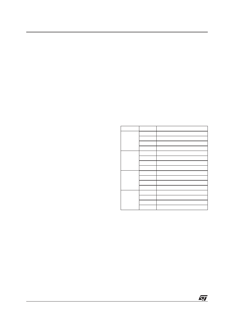
STD Timer Register
Register Address
STIM0
STH0
R240 (F0h)
STL0
R241 (F1h)
STP0
R242 (F2h)
STC0
R243 (F3h)
STIM1
STH1
R244 (F4h)
STL1
R245 (F5h)
STP1
R246 (F6h)
STC1
R247 (F7h)
STIM2
STH2
R248 (F8h)
STL2
R249 (F9h)
STP2
R250 (FAh)
STC2
R251 (FBh)
STIM3
STH3
R252 (FCh)
STL3
R253 (FDh)
STP3
R254 (FEh)
STC3
R255 (FFh)
9
相关PDF资料 |
PDF描述 |
|---|---|
| ST92F120R1Q6 | 16-BIT, FLASH, 24 MHz, MICROCONTROLLER, PQFP64 |
| ST92F120JR1Q7 | 16-BIT, FLASH, 24 MHz, MICROCONTROLLER, PQFP64 |
| ST92F150CV1Q6 | 16-BIT, FLASH, 24 MHz, MICROCONTROLLER, PQFP100 |
| ST92F150JDV1T6 | 16-BIT, FLASH, 24 MHz, MICROCONTROLLER, PQFP100 |
| ST92F150CV1T6 | 16-BIT, FLASH, 24 MHz, MICROCONTROLLER, PQFP100 |
相关代理商/技术参数 |
参数描述 |
|---|---|
| ST92F120V1Q7 | 功能描述:8位微控制器 -MCU Flash 128K SPI/I2C RoHS:否 制造商:Silicon Labs 核心:8051 处理器系列:C8051F39x 数据总线宽度:8 bit 最大时钟频率:50 MHz 程序存储器大小:16 KB 数据 RAM 大小:1 KB 片上 ADC:Yes 工作电源电压:1.8 V to 3.6 V 工作温度范围:- 40 C to + 105 C 封装 / 箱体:QFN-20 安装风格:SMD/SMT |
| ST92F120V9Q7 | 功能描述:8位微控制器 -MCU RO 511-ST92F150CV1QB RoHS:否 制造商:Silicon Labs 核心:8051 处理器系列:C8051F39x 数据总线宽度:8 bit 最大时钟频率:50 MHz 程序存储器大小:16 KB 数据 RAM 大小:1 KB 片上 ADC:Yes 工作电源电压:1.8 V to 3.6 V 工作温度范围:- 40 C to + 105 C 封装 / 箱体:QFN-20 安装风格:SMD/SMT |
| ST92F124R9TB | 功能描述:8位微控制器 -MCU Flash 64K SCI/SPI/I2 RoHS:否 制造商:Silicon Labs 核心:8051 处理器系列:C8051F39x 数据总线宽度:8 bit 最大时钟频率:50 MHz 程序存储器大小:16 KB 数据 RAM 大小:1 KB 片上 ADC:Yes 工作电源电压:1.8 V to 3.6 V 工作温度范围:- 40 C to + 105 C 封装 / 箱体:QFN-20 安装风格:SMD/SMT |
| ST92F124V1QB | 功能描述:8位微控制器 -MCU Flash 128K 2SCI/SPI RoHS:否 制造商:Silicon Labs 核心:8051 处理器系列:C8051F39x 数据总线宽度:8 bit 最大时钟频率:50 MHz 程序存储器大小:16 KB 数据 RAM 大小:1 KB 片上 ADC:Yes 工作电源电压:1.8 V to 3.6 V 工作温度范围:- 40 C to + 105 C 封装 / 箱体:QFN-20 安装风格:SMD/SMT |
| ST92F124V1T6 | 功能描述:8位微控制器 -MCU 8/16-BIT SINGLE VOLT RoHS:否 制造商:Silicon Labs 核心:8051 处理器系列:C8051F39x 数据总线宽度:8 bit 最大时钟频率:50 MHz 程序存储器大小:16 KB 数据 RAM 大小:1 KB 片上 ADC:Yes 工作电源电压:1.8 V to 3.6 V 工作温度范围:- 40 C to + 105 C 封装 / 箱体:QFN-20 安装风格:SMD/SMT |
发布紧急采购,3分钟左右您将得到回复。