- 您现在的位置:买卖IC网 > PDF目录98149 > STPCI2HEYI (STMICROELECTRONICS) MULTIFUNCTION PERIPHERAL, PBGA516 PDF资料下载
参数资料
| 型号: | STPCI2HEYI |
| 厂商: | STMICROELECTRONICS |
| 元件分类: | 外设及接口 |
| 英文描述: | MULTIFUNCTION PERIPHERAL, PBGA516 |
| 封装: | PLASTIC, BGA-516 |
| 文件页数: | 102/109页 |
| 文件大小: | 2430K |
| 代理商: | STPCI2HEYI |
第1页第2页第3页第4页第5页第6页第7页第8页第9页第10页第11页第12页第13页第14页第15页第16页第17页第18页第19页第20页第21页第22页第23页第24页第25页第26页第27页第28页第29页第30页第31页第32页第33页第34页第35页第36页第37页第38页第39页第40页第41页第42页第43页第44页第45页第46页第47页第48页第49页第50页第51页第52页第53页第54页第55页第56页第57页第58页第59页第60页第61页第62页第63页第64页第65页第66页第67页第68页第69页第70页第71页第72页第73页第74页第75页第76页第77页第78页第79页第80页第81页第82页第83页第84页第85页第86页第87页第88页第89页第90页第91页第92页第93页第94页第95页第96页第97页第98页第99页第100页第101页当前第102页第103页第104页第105页第106页第107页第108页第109页
STPC ATLAS
92/109
Issue 1.1 - March 23, 2004
6.4.3. MEMORY INTERFACE
6.4.3.1. Introduction
In order to achieve SDRAM memory interfaces
which work at clock frequencies of 90 MHz and
above, careful consideration has to be given to the
timing of the interface with all the various electrical
and physical constraints taken into consideration.
The guidelines described below are related to
SDRAM components on DIMM modules. For
applications where the memories are directly
soldered to the motherboard, the PCB should be
laid out such that the trace lengths fit within the
constraints shown here. The traces could be
slightly shorter since the extra routing on the
DIMM PCB is no longer present but it is then up to
the user to verify the timings.
6.4.3.2. SDRAM Clocking Scheme
The SDRAM Clocking Scheme deserves a special
mention here. Basically the memory clock is
generated on-chip through a PLL and goes
directly to the MCLKO output pin of the STPC. The
nominal frequency is 90 MHz. Because of the high
load presented to the MCLK on the board by the
DIMMs it is recommended to rebuffer the MCLKO
signal on the board and balance the skew to the
clock ports of the different DIMMs and the MCLKI
input pin of STPC.
6.4.3.3. Board Layout Issues
The physical layout of the motherboard PCB
assumed in this presentation is as shown in Figure
6-22. Because all of the memory interface signal
balls are located in the same region of the STPC
device, it is possible to orientate the device to
reduce the trace lengths. The worst case routing
length to the DIMM1 is estimated to be 100 mm.
Solid power and ground planes are a must in order
to provide good return paths for the signals and to
reduce EMI and noise. Also there should be ample
high frequency decoupling between the power
and ground planes to provide a low impedance
path between the planes for the return paths for
signal routings which change layers. If possible,
the traces should be routed adjacent to the same
power or ground plane for the length of the trace.
For the SDRAM interface, the most critical signal
is the clock. Any skew between the clocks at the
SDRAM components and the memory controller
will impact the timing budget. In order to get well
matched
clocks
at
all
components
it
is
recommended that all the DIMM clock pins, STPC
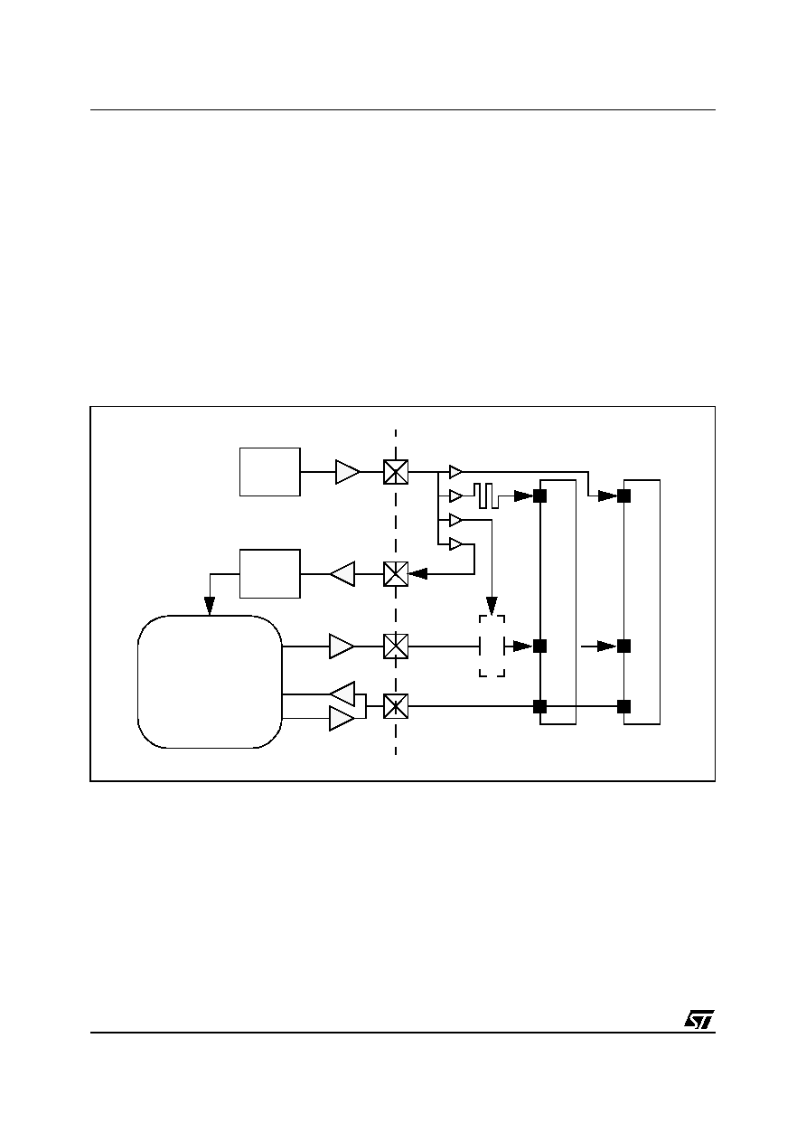
Figure 6-21. Clock Scheme
DIMM1
MCLKI
MCLKO
DIMM2
PLL
regi
s
ter
PLL
MA[ ] + Control
MD[63:0]
SDRAM
CONTROLLER
相关PDF资料 |
PDF描述 |
|---|---|
| STPCI2HDYC | MULTIFUNCTION PERIPHERAL, PBGA516 |
| STPIC6C595M | 8-BIT RIGHT SERIAL IN PARALLEL OUT SHIFT REGISTER, TRUE OUTPUT, PDSO16 |
| STR710RZT6 | 32-BIT, FLASH, 66 MHz, RISC MICROCONTROLLER, PQFP144 |
| STUF32864EHLFT | SSTU SERIES, POSITIVE EDGE TRIGGERED D FLIP-FLOP, TRUE OUTPUT, PBGA96 |
| STV3208CV | 9-BIT, DSP-FAST COSINE TRANSFRM PROCESSOR, PQFP44 |
相关代理商/技术参数 |
参数描述 |
|---|---|
| STPCINDUSTRIAL | 制造商:STMICROELECTRONICS 制造商全称:STMicroelectronics 功能描述:PC Compatible Embedded Microprocessor |
| STP-CN04 | 功能描述:烙铁 Cartridge Conical 0.4mm (0.016in) RoHS:否 制造商:Weller 产品:Soldering Stations 类型:Digital, Iron, Stand, Cleaner 瓦特:50 W 最大温度:+ 850 F 电缆类型:US Cord Included |
| STP-CN05 | 功能描述:烙铁 Cartridge Conical 0.5mm (0.02in) RoHS:否 制造商:Weller 产品:Soldering Stations 类型:Digital, Iron, Stand, Cleaner 瓦特:50 W 最大温度:+ 850 F 电缆类型:US Cord Included |
| STP-CN10 | 功能描述:烙铁 Cartridge Conical 1mm (0.039in) RoHS:否 制造商:Weller 产品:Soldering Stations 类型:Digital, Iron, Stand, Cleaner 瓦特:50 W 最大温度:+ 850 F 电缆类型:US Cord Included |
| STP-CNB04 | 功能描述:烙铁 Cartridge Conical Bent 0.4mm (0.016in) RoHS:否 制造商:Weller 产品:Soldering Stations 类型:Digital, Iron, Stand, Cleaner 瓦特:50 W 最大温度:+ 850 F 电缆类型:US Cord Included |
发布紧急采购,3分钟左右您将得到回复。