参数资料
| 型号: | SY69753LHI |
| 厂商: | Micrel Inc |
| 文件页数: | 11/13页 |
| 文件大小: | 0K |
| 描述: | IC CLOCK/DATA REC 155MBPS 32TQFP |
| 标准包装: | 250 |
| 类型: | 时钟和数据恢复(CDR),多路复用器 |
| PLL: | 是 |
| 主要目的: | 以太网,SONET/SDH,ATM OC-3 |
| 输入: | PECL |
| 输出: | PECL |
| 电路数: | 1 |
| 比率 - 输入:输出: | 1:3 |
| 差分 - 输入:输出: | 是/是 |
| 频率 - 最大: | 155Mbps |
| 电源电压: | 3.15 V ~ 3.45 V |
| 工作温度: | -40°C ~ 85°C |
| 安装类型: | 表面贴装 |
| 封装/外壳: | 32-TQFP 裸露焊盘 |
| 供应商设备封装: | 32-EPAD-TQFP |
| 包装: | 托盘 |
2012 Microchip Technology Inc.
Preliminary
DS22292A-page 7
MCP7940M
3.0
I2C BUS CHARACTERISTICS
3.1
I2C Interface
The MCP7940M supports a bidirectional 2-wire bus
and data transmission protocol. A device that sends
data onto the bus is defined as transmitter, and a
device receiving data as receiver. The bus has to be
controlled by a master device which generates the Start
and Stop conditions, while the MCP7940M works as
slave. Both master and slave can operate as
transmitter or receiver but the master device
determines which mode is activated.
3.1.1
BUS CHARACTERISTICS
The following bus protocol has been defined:
Data transfer may be initiated only when the bus
is not busy.
During data transfer, the data line must remain
stable whenever the clock line is high. Changes in
the data line while the clock line is high will be
interpreted as a Start or Stop condition.
Accordingly, the following bus conditions have been
defined (Figure 3-1).
3.1.1.1
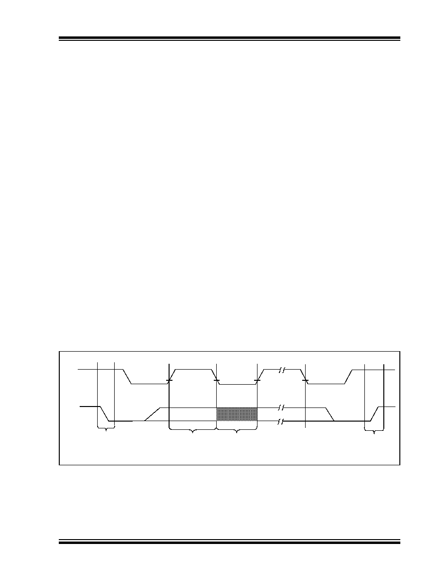
Bus not Busy (A)
Both data and clock lines remain high.
3.1.1.2
Start Data Transfer (B)
A high-to-low transition of the SDA line while the clock
(SCL) is high determines a Start condition. All
commands must be preceded by a Start condition.
3.1.1.3
Stop Data Transfer (C)
A low-to-high transition of the SDA line while the clock
(SCL) is high determines a Stop condition. All
operations must end with a Stop condition.
3.1.1.4
Data Valid (D)
The state of the data line represents valid data when,
after a Start condition, the data line is stable for the
duration of the high period of the clock signal.
The data on the line must be changed during the low
period of the clock signal. There is one bit of data per
clock pulse.
Each data transfer is initiated with a Start condition and
terminated with a Stop condition. The number of the
data bytes transferred between the Start and Stop
conditions is determined by the master device.
3.1.1.5
Acknowledge
Each receiving device, when addressed, is obliged to
generate an Acknowledge signal after the reception of
each byte. The master device must generate an extra
clock pulse which is associated with this Acknowledge
bit.
A device that acknowledges must pull down the SDA
line during the Acknowledge clock pulse in such a way
that the SDA line is stable-low during the high period of
the Acknowledge-related clock pulse. Of course, setup
and hold times must be taken into account. During
reads, a master must signal an end of data to the slave
by NOT generating an Acknowledge bit on the last byte
that has been clocked out of the slave. In this case, the
slave (MCP7940M) will leave the data line high to
enable the master to generate the Stop condition.
FIGURE 3-1:
DATA TRANSFER SEQUENCE ON THE SERIAL BUS
Address or
Acknowledge
Valid
Data
Allowed
to Change
Stop
Condition
Start
Condition
SCL
SDA
(A)
(B)
(D)
(C)
(A)
相关PDF资料 |
PDF描述 |
|---|---|
| VE-J6D-MW-B1 | CONVERTER MOD DC/DC 85V 100W |
| D38999/26FJ19SA | CONN PLUG 19POS STRAIGHT W/SCKT |
| VE-J61-MW-B1 | CONVERTER MOD DC/DC 12V 100W |
| D38999/24KA98SN | CONN RCPT 3POS JAM NUT W/SCKT |
| MS3452L14S-6S | CONN RCPT 6POS BOX MNT W/SCKT |
相关代理商/技术参数 |
参数描述 |
|---|---|
| SY69753LHI TR | 功能描述:IC CLOCK/DATA RECVRY 3.3V 32TQFP RoHS:否 类别:集成电路 (IC) >> 时钟/计时 - 专用 系列:- 标准包装:1,500 系列:- 类型:时钟缓冲器/驱动器 PLL:是 主要目的:- 输入:- 输出:- 电路数:- 比率 - 输入:输出:- 差分 - 输入:输出:- 频率 - 最大:- 电源电压:3.3V 工作温度:0°C ~ 70°C 安装类型:表面贴装 封装/外壳:28-SSOP(0.209",5.30mm 宽) 供应商设备封装:28-SSOP 包装:带卷 (TR) 其它名称:93786AFT |
| SY69753LHITR | 制造商:MICREL 制造商全称:Micrel Semiconductor 功能描述:3.3V, 125Mbps, 155Mbps Clock and Data Recovery |
| SY69753LHYTR | 制造商:Micrel Inc 功能描述:3.3V,125MBPS, 155MBPS CLOCK AND DATA RECOVERY |
| SY69754AL | 制造商:MICREL 制造商全称:Micrel Semiconductor 功能描述:3.3V, 622Mbps Clock and Data Recovery |
| SY69754AL_07 | 制造商:MICREL 制造商全称:Micrel Semiconductor 功能描述:3.3V, 622Mbps Clock and Data Recovery |
发布紧急采购,3分钟左右您将得到回复。