参数资料
| 型号: | SY89229UMG |
| 厂商: | Micrel Inc |
| 文件页数: | 13/16页 |
| 文件大小: | 0K |
| 描述: | IC CLK DIVIDER /3/5 LVDS 16-MLF |
| 标准包装: | 100 |
| 系列: | Precision Edge® |
| 类型: | 时钟除法器 |
| PLL: | 无 |
| 输入: | CML,LVDS,PECL |
| 输出: | LVDS |
| 电路数: | 1 |
| 比率 - 输入:输出: | 1:1 |
| 差分 - 输入:输出: | 是/是 |
| 频率 - 最大: | 1GHz |
| 除法器/乘法器: | 是/无 |
| 电源电压: | 2.375 V ~ 2.625 V |
| 工作温度: | -40°C ~ 85°C |
| 安装类型: | 表面贴装 |
| 封装/外壳: | 16-VFQFN 裸露焊盘,16-MLF? |
| 供应商设备封装: | 16-MLF?(3x3) |
| 包装: | 管件 |
| 产品目录页面: | 1083 (CN2011-ZH PDF) |
| 其它名称: | 576-1651-5 |
Micrel, Inc.
SY89229U
August 2007
M9999-080707-A
hbwhelp@micrel.com or (408) 955-1690
6
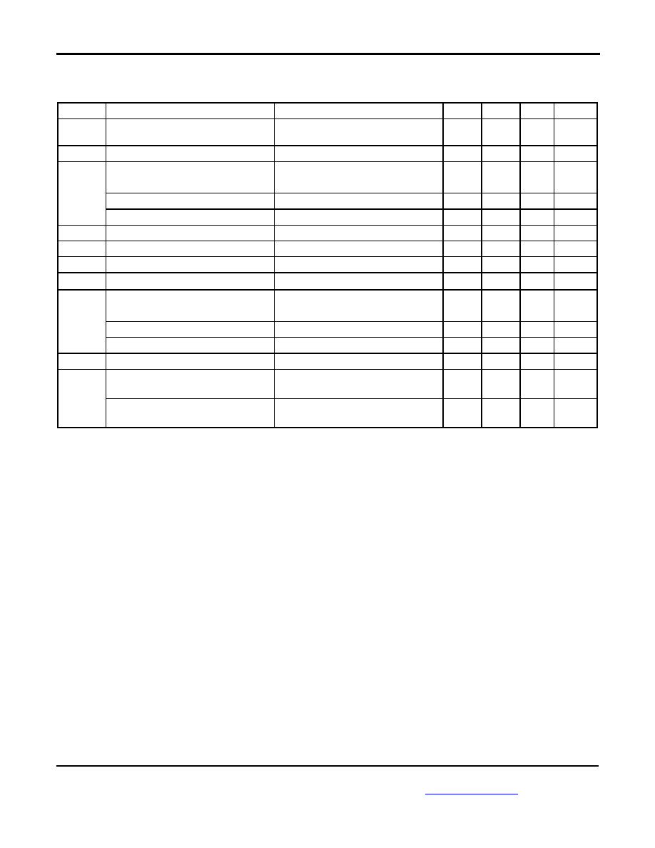
AC Electrical Characteristics
(8)
VCC = 2.5V ±5%; RL = 100
across the outputs; T
A = –40°C to + 85°C, unless otherwise stated.
Symbol
Parameter
Condition
Min
Typ
Max
Units
fMAX
Maximum Input Operating
Frequency
VOUT
≥ 200mV
1.0
1.5
GHz
tw
Minimum Pulse Width
IN, /IN
400
ps
tpd
Differential Propagation Delay
In-to-Q
100mV < VIN
≤ 200mV, Note 9
900
1150
1500
ps
In-to-Q
200mV < VIN
≤ 800mV, Note 9
800
1050
1400
ps
/MR(H-L)-to-Q
350
530
800
ps
tRR
Reset Recovery Time
/MR(L-H)-to-IN
400
ps
tS EN
Set-up Time
EN-to-IN
Note 10
300
ps
tH EN
Hold Time
IN-to-EN
Note 10
800
ps
tskew
Part-to-Part Skew
Note 10
450
ps
tJITTER
Clock
Random Jitter
Note 11
1
psRMS
Cycle-to-Cycle Jitter
Note 12
1
psRMS
Total Jitter
Note 13
10
psPP
tr, tf
Output Rise/Fall Time (20% to 80%)
At full output swing.
100
220
ps
Output Duty Cycle(÷ 3)
Duty Cycle(input): 50%; f
≤1GHz;
Note 14
46
54
%
Output Duty Cycle(÷ 5)
Duty Cycle(input): 50%; f
≤1GHz;
Note 14
47
53
%
Notes:
8. High-frequency AC-parameters are guaranteed by design and characterization.
9. Propagation delay is measured with input tr, tf
≤ 300ps (20% to 80%). The propagation delay is function of the rise and fall times at IN. See
“Typical Operating Characteristics” for details.
10. Set-up and hold times apply to synchronous applications that intend to enable/disable before the next clock cycle. For asynchronous
applications, set-up and hold do not apply.
11. Random Jitter is measured with a K28.7 character pattern, measured at <fMAX.
12. Cycle-to-Cycle Jitter definition: the variation of periods between adjacent cycles, Tn – Tn-1 where T is the time between rising edges of the
output signal.
13. Total Jitter definition: with an ideal clock input of frequency <fMAX, no more than one output edge in 10
12 output edges will deviate by more
than the specified peak-to-peak jitter value.
14. For Input Duty Cycle different from 50%, see “Output Duty Cycle Equation” in “Functional Description” subsection.
相关PDF资料 |
PDF描述 |
|---|---|
| VE-27L-MW-S | CONVERTER MOD DC/DC 28V 100W |
| VE-BWB-MV-S | CONVERTER MOD DC/DC 95V 150W |
| VI-2T2-MY-F3 | CONVERTER MOD DC/DC 15V 50W |
| ADF4107BRU-REEL | IC PLL FREQ SYNTHESIZER 16-TSSOP |
| VI-2TX-IV | CONVERTER MOD DC/DC 5.2V 150W |
相关代理商/技术参数 |
参数描述 |
|---|---|
| SY89229UMG TR | 功能描述:时钟驱动器及分配 Divide-by-3 and 5 LVDS Clock Divider with Internal Termination and FSI (1GHz) RoHS:否 制造商:Micrel 乘法/除法因子:1:4 输出类型:Differential 最大输出频率:4.2 GHz 电源电压-最大: 电源电压-最小:5 V 最大工作温度:+ 85 C 封装 / 箱体:SOIC-8 封装:Reel |
| SY89229UMGTR | 制造商:MICREL 制造商全称:Micrel Semiconductor 功能描述:1GHz Precision, LVDS ÷3, ÷5 Clock Divider with Fail Safe Input and Internal Termination |
| SY89230U | 制造商:MICREL 制造商全称:Micrel Semiconductor 功能描述:1GHz Precision, LVPECL ±3, ±5 Clock Divider with Fail-Safe Input and Internal Termination |
| SY89230U_10 | 制造商:MICREL 制造商全称:Micrel Semiconductor 功能描述:3.2GHz Precision, LVPECL ÷3, ÷5 Clock Divider |
| SY89230U-EVAL | 制造商:Micrel Inc 功能描述:DIVIDE-BY-3 AND 5 LVPECL CLOCK |
发布紧急采购,3分钟左右您将得到回复。