参数资料
| 型号: | SY89297UMG TR |
| 厂商: | Micrel Inc |
| 文件页数: | 10/15页 |
| 文件大小: | 0K |
| 描述: | IC DELAY LINE 1024TAP 24-QFN |
| 标准包装: | 1,000 |
| 系列: | Precision Edge® |
| 标片/步级数: | 1024 |
| 功能: | 多重,可编程 |
| 延迟到第一抽头: | 2ns |
| 接头增量: | 5ps |
| 可用的总延迟: | 2ns ~ 7.5ns |
| 独立延迟数: | 2 |
| 电源电压: | 2.375 V ~ 3.6 V |
| 工作温度: | -40°C ~ 85°C |
| 安装类型: | 表面贴装 |
| 封装/外壳: | 24-VFQFN 裸露焊盘 |
| 供应商设备封装: | 24-QFN(4x4) |
| 包装: | 带卷 (TR) |
Micrel, Inc.
SY89297U
December 2011
4
M9999-120211-C
hbwhelp@micrel.com or (408) 955-1690
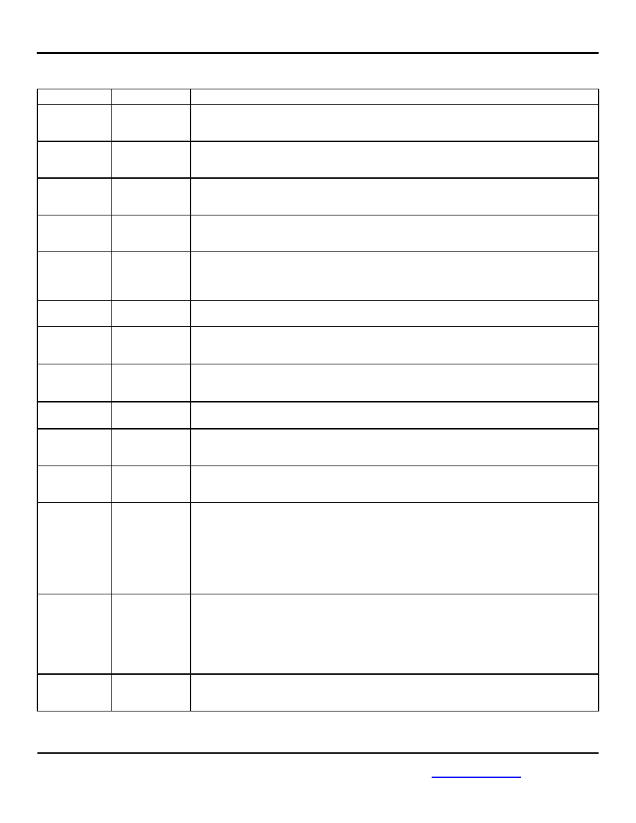
Pin Description
Pin Number
Pin Name
Pin Function
1
2
INA
/INA
Channel A Differential Input: INA and /INA pins receive the Channel A data. QA and /QA are
the delayed product of INA and /INA. Each input is internally terminated to VTA through a 50
resistor (100 across INA and /INA).
3
VTA
Input A Termination Center-Tap: Each side of the differential input pair terminates to this pin.
This pin provides a center-tap to a termination network for maximum interface flexibility. See
“Input Interface Applications” section.
4
VTB
Input B Termination Center-Tap: Each side of the differential input pair terminates to this pin.
This pin provides a center-tap to a termination network for maximum interface flexibility. See
“Input Interface Applications” section.
5
6
INB
/INB
Channel B Differential Input: INB and /INB pins receive the Channel B data. QB and /QB are
the delayed product of INB and /INB. Each input is internally terminated to VTB through a 50
resistor (100 across INB and /INB).
7
VREF-AC
Reference Voltage Output: For AC-coupled input signals, this pin can bias the inputs IN and /IN.
Connect VREF-AC directly to the VT input pin for each channel. De-couple to VCC using a
0.01F capacitor. Maximum sink/source current is
±0.5mA. For DC-coupled input applications,
leave VREF-AC pin floating.
8, 11, 20
GND,
Exposed Pad
Negative Supply: Exposed pad must be connected to a ground plane that is the same potential
as the ground pins.
9
/ENA
CMOS/TTL-Compatible Enable Input: When the /ENA pin is pulled HIGH, QA is held LOW and
/QA goes HIGH after the programmed delay propagates through the part. /ENA contains a
67k
Ω pull-down resistor and defaults LOW when left floating. Logic threshold level is VCC/2
10
/ENB
CMOS/TTL-Compatible Enable Input: When the /ENB pin is pulled HIGH, QB is held LOW and
/QB goes HIGH after the programmed delay propagates through the part. /ENB contains a
67k
Ω pull-down resistor and defaults LOW when left floating. Logic threshold level is Vcc/2
12, 15, 16, 19
VCC
Power Supply: Bypass each supply pin with 0.1F//0.01F low-ESR capacitors. See DC
Electrical Characteristics table for more details. 2.5V
±5% or 3.3V ±10%.
13
14
/QB
QB
CML Differential Output: QB and /QB are the delayed product of INB, /INB. CML outputs are
terminated at the destination with 100 across the pair. See “CML Output Termination”
section.
17
18
/QA
QA
CML Differential Output: QA and /QA are the delayed product of INA, /INA. CML outputs are
terminated at the destination with 100 across the pair. See “CML Output Termination”
section.
23
22
SCLK
SDATA
CMOS/TTL-compatible 3-pin serial programming control inputs: The 3-pin serial control sets
each channel’s IN to Q delay. DA(0:9) control channel A delay. DB(0:9) control channel B. To
program the two channels, insert a 20-bit word (DA0:DA9 and DB0:DB9) into SDATA and clock
in the control bits with SCLK. Maximum input frequency to SCLK is 40MHz. Data is loaded into
the serial registers on the L-H transition of SCLK. After all 20-bits are clocked in, SLOAD
latches the new delay bits. These pins have internal pull-downs at the inputs. See “AC
Electrical Characteristics” for delay values. Logic threshold level is Vcc/2. SCLK and SDATA
contain a 67k
Ω pull-down resistor and default LOW when left floating.
24
SLOAD
CMOS/TTL-compatible 3-pin serial programming control input: SLOAD controls the latches that
transfer scanned data to the delay line. These latches are transparent when SLOAD is high.
Data transfers from the latch to the delay line on a L-H transition of SLOAD. SLOAD has to
transition H-L before new data is loaded in the scan chain. When SLOAD is high, the latches
are transparent and SCLK cannot switch. Otherwise, new data will immediately transfer to the
scan chain. Logic threshold level is Vcc/2. SLOAD contains a 67k pull-down resistor and
defaults LOW when left floating.
21
SOUT
CMOS/TTL-compatible output: This pin is used to support cascading multiple SY89297U delay
lines. Serial data is clocked into the SDATA input and is clocked out of SOUT into the next
SY89297U delay line. SOUT pin includes an internal 550 pull-up resistor.
相关PDF资料 |
PDF描述 |
|---|---|
| D38999/26MB98PB | CONN PLUG 6POS STRAIGHT W/PINS |
| VI-2WK-MW | CONVERTER MOD DC/DC 40V 100W |
| MS3121F14-12P | CONN RCPT 12POS CBL MNT W/PINS |
| AD5271BRMZ-100 | IC RHEOSTAT 5V 50-TP 256 10MSOP |
| SY89296UMG TR | IC DELAY LINE 1024TAP 32-MLF |
相关代理商/技术参数 |
参数描述 |
|---|---|
| SY89297UMH | 功能描述:延迟线/计时元素 2.5V Dual Channel Delay Line with 5ps Step Delay (improved SY89295) RoHS:否 制造商:Micrel 功能:Active Programmable Delay Line 传播延迟时间:1000 ps 工作温度范围: 封装 / 箱体:QFN-24 封装:Tube |
| SY89297UMH TR | 功能描述:延迟线/计时元素 2.5V Dual Channel Delay Line with 5ps Step Delay (improved SY89295) RoHS:否 制造商:Micrel 功能:Active Programmable Delay Line 传播延迟时间:1000 ps 工作温度范围: 封装 / 箱体:QFN-24 封装:Tube |
| SY89306 | 制造商:MICREL 制造商全称:Micrel Semiconductor 功能描述:3.3V/5V 2.5GHz PECL/ECL DIFFERENTIAL RECEIVER/BUFFER |
| SY89306_06 | 制造商:MICREL 制造商全称:Micrel Semiconductor 功能描述:3.3V/5V 2.5GHz PECL/ECL DIFFERENTIAL RECEIVER/BUFFER |
| SY89306V | 制造商:MICREL 制造商全称:Micrel Semiconductor 功能描述:3.3V / 5V 2.5 GHZ PECL/ECL DIFFERENTIAL RECEIVER/BUFFER |
发布紧急采购,3分钟左右您将得到回复。