- 您现在的位置:买卖IC网 > PDF目录98150 > SY89482LMGTR (MICREL INC) LOW SKEW CLOCK DRIVER, QCC24 PDF资料下载
参数资料
| 型号: | SY89482LMGTR |
| 厂商: | MICREL INC |
| 元件分类: | 时钟及定时 |
| 英文描述: | LOW SKEW CLOCK DRIVER, QCC24 |
| 封装: | 4 X 4 MM, LEAD FREE, MLF-24 |
| 文件页数: | 11/16页 |
| 文件大小: | 425K |
| 代理商: | SY89482LMGTR |
Micrel, Inc.
SY89482L
April 2008
4
M9999-040808-A
hbwhelp@micrel.com or (408) 955-1690
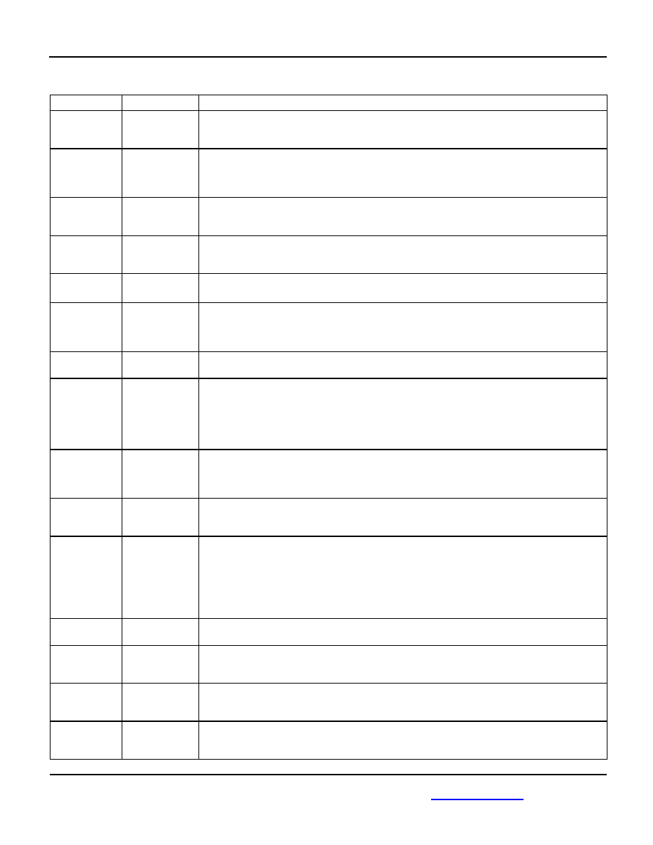
Pin Description
Pin Number
Pin Name
Pin Function
1
VT
Input Termination Center-Tap: Each side of the differential input pair terminates to VT pin.
This pin provides a center-tap to a termination network for maximum interface flexibility. See
“Input Interface Applications” subsection.
2
VREF-AC
Reference Output Voltage: This output biases to VDD-1.4V. It is used when AC-coupling the
inputs (IN, /IN). Connect VREF-AC directly to the VT pin. Bypass with 0.01uF low ESR
capacitors to VDD. Maximum current source or sink is ±0.5mA. See “Input Interface
Applications” subsection.
3, 4
REFIN,
/REFIN
Differential Input Pair: This input pair is the differential signal input to the device. Input
accepts AC- or DC-coupled differential signals as small as 100mV (200mVpp). Each pin of
this pair internally terminates with 50
to the VT pin. See Figure 2a.
12
/EN
Single-ended Input: This TTL/CMOS input disables and enables the output. It has an internal
pull-down and will default to a logic LOW state if left open. When HIGH, the output is forced
into the disable state (Q = LOW and /Q = HIGH). The pull-down current is typically 0.5A.
6, 13
GND,
Exposed Pad
Ground: These are the ground pins for core and input stage. Exposed pad must be
connected to a ground plane that is the same potential as the ground pin.
9, 10
CLKOUT,
/CLKOUT
CML Differential Output Pair: Differential buffered output copy of the input signal with very
low jitter. The output swing is typically 400mV. The output pair is referenced to VDDO. Output
pair can be terminated 100
across or 50 to VBIAS. See “CML Output Termination”
subsection. See Figure 2b.
7
GNDO
Ground: This is the ground pin for output stage. GNDO and GND must be connected
together on the PCB.
8, 11
VDDO
CML Output Driver Power Pins: VDDO enables the output stage to operate from a lower
supply voltage than the core synthesizer voltage. These outputs can be powered from 1.8V
±5% to 3.3V ±10% power supply. For applications that only require 3.3V reference output
operation, VDDO and VDD pins may be connected to a common power supply. Connect both
VDDO pins to same power supply. Bypass with 0.1uF//0.01uF low ESR capacitors as close
to the VDD pins as possible.
15
RESET
Single-ended Input: Reset is active on the Low-to-High edge of the input pulse. It has an
internal pull-down and will default to a logic LOW state if left open. Resetting the part starts
an auto-tune sequence to provide output frequency closest to input frequency. Calibration
setting is lost on power down. The pull-down current is typically 0.5A.
14
LOL
Single-ended Output: This LVTTL/CMOS output asserts HIGH when the PLL is out of phase
lock. LOL is asserted if the PLL frequency deviates more than ±1000ppm for more than 5ms.
This prevents false triggering. The Loss of Lock pin can be directly connected to /EN.
20, 21
FILTERN,
FILTERP
Analog Input: These pins provide reference for PLL loop filter. Connect a LOW ESR capacitor
across these pins as close to the device as possible, clear from any supply lines or adjacent
signal lines. See “External Loop Filter Considerations” for loop filter values. Loop filter
capacitor value depends on I/O frequency selection. Loop filter capacitor layout should
include a quiet ground plane under the loop filter capacitor and loop filter (FILTERP,
FILTERN) pins. Recommend 1206, X5R, 6.3V ceramic type, +/-30%. See “PLL Loop Filter
Capacitor Table”.
18, 23
GNDA
Ground: This is an analog ground pin for the PLL. Connect to “quiet” ground. It is internally
referenced to the VCO. GNDA and Ground must be shorted on the PCB.
19, 22
VDDA
Analog Power: Connect to “quiet” 3.3V ±10% power supply. These pins are not internally
connected and must be shorted on the PCB. VDDA internally connects to the VCO. Bypass
with 0.1F//0.01F low ESR capacitors as close to the pin as possible
16, 17
BW0, BW1
Single-ended Input: These LVTTL/CMOS inputs determine the loop bandwidth of the jitter
reducing PLL. BWSEL0 and BWSEL1 will default to a logic HIGH state if left open with a
typical pull-up current of 1.3A. See “Loop Bandwidth Table.”
5, 24
VDDC
Positive Power Supply: VDDC pins are connected to core and input stage that connects to a
3.3V ±10% power supply. Bypass with 0.1F//0.01F low ESR capacitors as close to the VCC
pins as possible.
相关PDF资料 |
PDF描述 |
|---|---|
| SY89531LHZ | 622.08 MHz, OTHER CLOCK GENERATOR, PQFP64 |
| SY89534LHZ | 89534 SERIES, PLL BASED CLOCK DRIVER, 13 TRUE OUTPUT(S), 0 INVERTED OUTPUT(S), PQFP64 |
| SY89534LHZTR | 89534 SERIES, PLL BASED CLOCK DRIVER, 13 TRUE OUTPUT(S), 0 INVERTED OUTPUT(S), PQFP64 |
| SY89536LHZ | 89536 SERIES, PLL BASED CLOCK DRIVER, 13 TRUE OUTPUT(S), 0 INVERTED OUTPUT(S), PQFP64 |
| SY89537LMHTR | 756 MHz, OTHER CLOCK GENERATOR, QCC44 |
相关代理商/技术参数 |
参数描述 |
|---|---|
| SY89529L | 制造商:MICREL 制造商全称:Micrel Semiconductor 功能描述:3.3V 200MHz PRECISION SPREADSPECTRUM CLOCK SYNTHESIZER |
| SY89529LTC | 功能描述:IC SYNTHESIZER CLK 200MHZ 32TQFP RoHS:否 类别:集成电路 (IC) >> 时钟/计时 - 时钟发生器,PLL,频率合成器 系列:Precision Edge® 产品变化通告:Product Discontinuation 04/May/2011 标准包装:96 系列:- 类型:时钟倍频器,零延迟缓冲器 PLL:带旁路 输入:LVTTL 输出:LVTTL 电路数:1 比率 - 输入:输出:1:8 差分 - 输入:输出:无/无 频率 - 最大:133.3MHz 除法器/乘法器:是/无 电源电压:3 V ~ 3.6 V 工作温度:0°C ~ 70°C 安装类型:表面贴装 封装/外壳:16-TSSOP(0.173",4.40mm 宽) 供应商设备封装:16-TSSOP 包装:管件 其它名称:23S08-5HPGG |
| SY89529LTCTR | 制造商:MICREL 制造商全称:Micrel Semiconductor 功能描述:3.3V 200MHz PRECISION SPREADSPECTRUM CLOCK SYNTHESIZER |
| SY89529LTH | 功能描述:IC SYNTHESIZER CLK 200MHZ 32TQFP RoHS:是 类别:集成电路 (IC) >> 时钟/计时 - 时钟发生器,PLL,频率合成器 系列:Precision Edge® 产品变化通告:Product Discontinuation 04/May/2011 标准包装:96 系列:- 类型:时钟倍频器,零延迟缓冲器 PLL:带旁路 输入:LVTTL 输出:LVTTL 电路数:1 比率 - 输入:输出:1:8 差分 - 输入:输出:无/无 频率 - 最大:133.3MHz 除法器/乘法器:是/无 电源电压:3 V ~ 3.6 V 工作温度:0°C ~ 70°C 安装类型:表面贴装 封装/外壳:16-TSSOP(0.173",4.40mm 宽) 供应商设备封装:16-TSSOP 包装:管件 其它名称:23S08-5HPGG |
| SY89529LTH TR | 功能描述:IC SYNTHESIZER CLK 200MHZ 32TQFP RoHS:是 类别:集成电路 (IC) >> 时钟/计时 - 时钟发生器,PLL,频率合成器 系列:Precision Edge® 产品变化通告:Product Discontinuation 04/May/2011 标准包装:96 系列:- 类型:时钟倍频器,零延迟缓冲器 PLL:带旁路 输入:LVTTL 输出:LVTTL 电路数:1 比率 - 输入:输出:1:8 差分 - 输入:输出:无/无 频率 - 最大:133.3MHz 除法器/乘法器:是/无 电源电压:3 V ~ 3.6 V 工作温度:0°C ~ 70°C 安装类型:表面贴装 封装/外壳:16-TSSOP(0.173",4.40mm 宽) 供应商设备封装:16-TSSOP 包装:管件 其它名称:23S08-5HPGG |
发布紧急采购,3分钟左右您将得到回复。