参数资料
| 型号: | SY89823LHY |
| 厂商: | Micrel Inc |
| 文件页数: | 2/8页 |
| 文件大小: | 0K |
| 描述: | IC CLK BUF MUX TRNSL 2:22 64TQFP |
| 标准包装: | 160 |
| 系列: | Precision Edge® |
| 类型: | 扇出缓冲器(分配),多路复用器,变换器 |
| 电路数: | 1 |
| 比率 - 输入:输出: | 2:22 |
| 差分 - 输入:输出: | 是/是 |
| 输入: | HSTL,LVPECL |
| 输出: | HSTL |
| 频率 - 最大: | 500MHz |
| 电源电压: | 3.15 V ~ 3.45 V |
| 工作温度: | -40°C ~ 85°C |
| 安装类型: | 表面贴装 |
| 封装/外壳: | 64-TQFP 裸露焊盘 |
| 供应商设备封装: | 64-EP-TQFP |
| 包装: | 托盘 |
| 产品目录页面: | 1083 (CN2011-ZH PDF) |
| 其它名称: | 576-2090 SY89823LHY-ND |
2
Precision Edge
SY89823L
Micrel, Inc.
M9999-091908
hbwhelp@micrel.com or (408) 955-1690
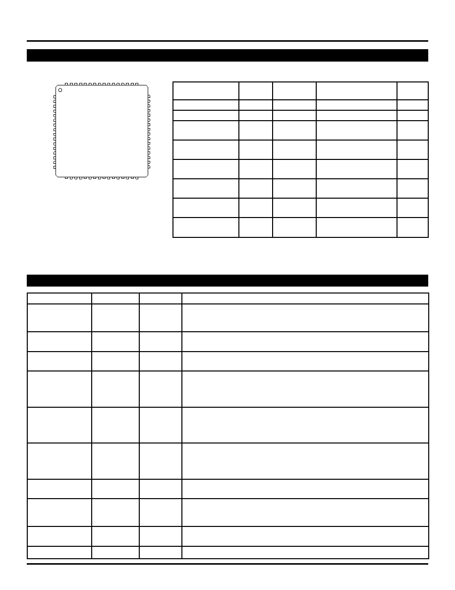
PACKAGE/ORDERING INFORMATION
Q1
VCCO
Q6
Q5
Q4
Q3
Q2
Q1
Q0
VCCO
NC
VCCI
HSTL_CLK
/HSTL_CLK
CLK_SEL
LVPECL_CLK
/LVPECL_CLK
GND
OE
NC
/Q21
Q21
VCCO
Q7
/Q7
Q8
/Q8
Q9
/Q9
Q10
/Q10
Q11
/Q11
Q12
/Q12
Q13
/Q13
VCCO
64
1
2
3
4
5
6
7
8
9
10
11
12
13
14
15
16
48
47
46
45
44
43
42
41
40
39
38
37
36
35
34
33
63 62 61 60 59 58 57 56 55 54 53 52 51 50 49
17 18 19 20 21 22 23 24 25 26 27 28 29 30 31 32
/Q19
VCCO
Q14
/Q14
Q15
/Q15
Q16
/Q16
Q17
/Q17
Q18
/Q18
Q19
Q20
/Q20
VCCO
64-Pin EPAD-TQFP (H64-1)
PIN DESCRIPTION
Pin Number
Pin Name
Type
Pin Function
5, 6
HSTL_CLK,
HSTL
Differential clock input selected by CLK_SEL. Can be left floating if not selected. Floating
/HSTL_CLK
Input
input, if selected, produces an indeterminate output. HSTL input signal requires external
termination 50
to GND.
8, 9
LVPECL_CLK,
LVPECL
Differential clock input selected by CLK_SEL. Can be left floating. Floating input, if
/LVPECL_CLK
Input
selected, produces a LOW at the output. Requires external termination. 75k
pull-up.
7
CLK_SEL
LVTTL
Selects HSTL_CLK input when LOW and LVPECL_CLK output when HIGH. 11k
Input
pull-up. Default condition selects LVPECL_CLK if left open.
11
OE
LVTTL
Enable input synchronized internally to prevent glitching of the Q0-Q21 and /Q0–/Q21
Input
outputs. Must be a minimum of three clock periods wide if synchronous with the CLK
inputs and must meet the t
S and tH requirements (refer to “AC Electrical Characteristics”
section). If asynchronous, must be a minimum of four clock periods wide. 11k
pull-up.
63, 61, 59, 57, 55, 53
Q0–Q21
HSTL
Differential clock outputs from HSTL_CLK when CLK_SEL = LOW and LVPECL outputs
51, 47, 45, 43, 41, 39
Output
when CLK_SEL = HIGH. HSTL outputs must be terminated with 50
to GND. Q0–Q21
37, 35, 31, 29, 27
outputs are static LOW when OE = LOW. Unused output pairs may be left floating.
25, 23, 21, 19, 15
62, 60, 58, 56, 54, 52
/Q0–/Q21
HSTL
Differential clock outputs from HSTL_CLK when CLK_SEL = LOW and LVPECL outputs
50, 46, 44, 42, 40, 38
Output
when CLK_SEL = HIGH. HSTL outputs must be terminated with 50
to GND. /Q0–/Q21
36, 34, 30, 28, 26
outputs are static HIGH when OE = LOW. Unused output pairs may be left floating.
24, 22, 20, 18, 14
4
VCCI
VCC Core
Core V
CC connected to 3.3V supply. Bypass with 0.1F in parallel with Power 0.01F
low ESR capacitors as close to V
CCI pins as possible.
1, 16, 17, 32,
VCCO
VCC Output
Output Buffer V
CC connected to 1.8V supply. Bypass with 0.1F in parallel with 0.01F
33, 48, 49, 64
Power
low ESR capacitors as close to V
CCO pin as possible. All VCCO pins should be
connected together on the PCB.
10
GND,
Ground pin and exposed pad must be connected to the same ground plane.
Exposed Pad
2, 3, 12, 13
NC
No Connect.
Ordering Information(1)
Package
Operating
Package
Lead
Part Number
Type
Range
Marking
Finish
SY89823LHC
H64-1
Commercial
SY89823LHC
Sn-Pb
SY89823LHCTR(2)
H64-1
Commercial
SY89823LHC
Sn-Pb
SY89823LHZ(3)
H64-1
Commercial
SY89823LHZ with
Pb-Free
Pb-Free bar-line indicator
Matte-Sn
SY89823LHZTR(2, 3)
H64-1
Commercial
SY89823LHZ with
Pb-Free
Pb-Free bar-line indicator
Matte-Sn
SY89823LHI
H64-1
Industrial
SY89823LHI with
Sn-Pb
Pb-Free bar-line indicator
SY89823LHITR(2, 3)
H64-1
Industrial
SY89823LHI with
Sn-Pb
Pb-Free bar-line indicator
SY89823LHY(3)
H64-1
Industrial
SY89823LHY with
Pb-Free
Pb-Free bar-line indicator
Matte-Sn
SY89823LHYTR(2, 3)
H64-1
Industrial
SY89823LHY with
Pb-Free
Pb-Free bar-line indicator
Matte-Sn
Notes:
1. Contact factory for die availability. Dice are guaranteed at T
A = 25°C, DC electricals only.
2. Tape and Reel.
3. Pb-Free package recommended for new designs.
相关PDF资料 |
PDF描述 |
|---|---|
| LTC6993MPS6-1#TRMPBF | IC MULTIVIBRATOR MONO TSOT23-6 |
| LTC6993HS6-4#TRPBF | IC MONO MULTIVIBRATOR TSOT23-6 |
| D38999/26JJ8SNLC | CONN HSG PLUG 8POS STRGHT SCKT |
| D38999/26MJ8BN | CONN HSG PLUG 8POS STRGHT SCKT |
| ADCLK944BCPZ-R2 | IC CLOCK BUFFER 1:4 7GHZ 16LFCSP |
相关代理商/技术参数 |
参数描述 |
|---|---|
| SY89823LHY TR | 功能描述:时钟缓冲器 500MHz 1:22 Diff. HSTL Fanout Buffer (I Temp, Lead Free) RoHS:否 制造商:Texas Instruments 输出端数量:5 最大输入频率:40 MHz 传播延迟(最大值): 电源电压-最大:3.45 V 电源电压-最小:2.375 V 最大功率耗散: 最大工作温度:+ 85 C 最小工作温度:- 40 C 封装 / 箱体:LLP-24 封装:Reel |
| SY89823LHYTR | 制造商:MICREL 制造商全称:Micrel Semiconductor 功能描述:3.3V, 500MHz 1:22 DIFFERENTIAL HSTL (1.5V) FANOUT BUFFER/TRANSLATOR |
| SY89823LHZ | 制造商:MICREL 制造商全称:Micrel Semiconductor 功能描述:3.3V, 500MHz 1:22 DIFFERENTIAL HSTL (1.5V) FANOUT BUFFER/TRANSLATOR |
| SY89823LHZTR | 制造商:MICREL 制造商全称:Micrel Semiconductor 功能描述:3.3V, 500MHz 1:22 DIFFERENTIAL HSTL (1.5V) FANOUT BUFFER/TRANSLATOR |
| SY89824L | 制造商:MICREL 制造商全称:Micrel Semiconductor 功能描述:3.3V 1:22 HIGH-PERFORMANCE, LOW VOLTAGE BUS CLOCK DRIVER |
发布紧急采购,3分钟左右您将得到回复。