- 您现在的位置:买卖IC网 > PDF目录98150 > T4260ILS (ATMEL CORP) AUDIO TUNER, PDSO44 PDF资料下载
参数资料
| 型号: | T4260ILS |
| 厂商: | ATMEL CORP |
| 元件分类: | 调谐器 |
| 英文描述: | AUDIO TUNER, PDSO44 |
| 封装: | SSO-44 |
| 文件页数: | 14/30页 |
| 文件大小: | 299K |
| 代理商: | T4260ILS |
第1页第2页第3页第4页第5页第6页第7页第8页第9页第10页第11页第12页第13页当前第14页第15页第16页第17页第18页第19页第20页第21页第22页第23页第24页第25页第26页第27页第28页第29页第30页
21
T4260
4528I–AUDR–08/04
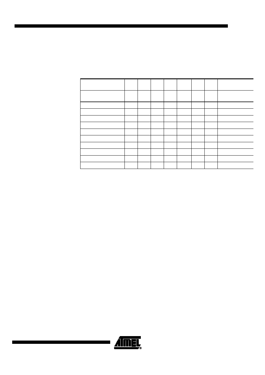
The offset of DAC1 and DAC2 has a range of approximately +0.98 V to -0.99 V. This
range is divided into 127 steps. One step is approximately 1.97 V/127 = 15.52 mV. The
offset of DAC1 can be controlled by the bits 24 to bit 30 (20 to 26) and the offset gain of
DAC2 can be controlled by the bits 52 to bit 58 (20 to 26) as given in Table 27.
Note:
Gain = 58 (intermediate position)
Permitted DAC Conditions
The internal operation amplifier of the DACs should not operate with a too high internal
difference voltage at their inputs. This means that a voltage difference higher than 0.5 V
at the internal OP input should be avoided in operation mode. The respective output OP
in the DAC is necessary for the addition and amplification of the tuning voltage (at
pin 18) with the desired voltage gain and offset value.
If the tuning voltage reaches a high value e.g. 9 V, with a gain setting of 2 times VTUNE
and an offset of +1 V, then the output OP of the DAC should reach the (calculated) volt-
age of 19 V. The supply voltage of e.g. 10 V, however, limits the output voltage (of the
DAC) to 10 V maximum.
Due to the (limiting) supply voltage and the internal gain resistance ratio of 6, the miss-
ing 9 V (calculated voltage - V
s) cause a voltage of 1.5 V at the OP input. This condition
may not remain for a longer period of time.
As long as the calculated DAC output voltage value does not exceed the supply voltage
value by more than 3 V, no damages should occur during the product’s lifetime as the
input voltage of the internal OP input voltage does not exceed 0.5 V.
VTUNE x DAC gain factor + DAC offset < V
S + 3 V
(9 V x 2 + 1 V) < 10 V + 3 V (condition not allowed)
This means when having a gain factor of 2 and an offset value of 1 V, the tuning voltage
should not exceed 6 V.
Maximum tuning voltage < (V
S + 3 V - DAC offset)/DAC gain factor
e.g.: maximum tuning voltage = (10 V + 3 V - 1 V)/2 = 6 V
It is also possible to reduce the gain or the offset value instead of (or along with) the tun-
ing voltage.
Table 27. Offset of DAC1, 2
Offset DAC1
Approximately
B30
B29
B28
B26
B25
B24
Decimal Offset
Offset DAC2
Approximately
B58
B57
B56
B55
B54
B53
B52
Decimal Offset
0.9815 V
0
0.9659 V
0
1
0.9512 V
0
1
0
2
0.9353 V
0
1
3
...
-0.0120 V
1
0
64
...
-0.9576 V
1
0
1
125
-0.9733 V
1
0
126
-0.9890 V
1
127
相关PDF资料 |
PDF描述 |
|---|---|
| T555200-PAE | SPECIALTY CONSUMER CIRCUIT, PXMA |
| T6B70BFNG | SPECIALTY ANALOG CIRCUIT, PDSO16 |
| T6F18 | SPECIALTY CONSUMER CIRCUIT, PQFP80 |
| T6N71B | SPECIALTY CONSUMER CIRCUIT, PQFP48 |
| T6N71QFP | SPECIALTY CONSUMER CIRCUIT, PQFP44 |
相关代理商/技术参数 |
参数描述 |
|---|---|
| T4260-ILSH | 功能描述:射频无线杂项 COM.RADIO-AM/FM FE DIG.CONCEPT RoHS:否 制造商:Texas Instruments 工作频率:112 kHz to 205 kHz 电源电压-最大:3.6 V 电源电压-最小:3 V 电源电流:8 mA 最大功率耗散: 工作温度范围:- 40 C to + 110 C 封装 / 箱体:VQFN-48 封装:Reel |
| T428P107M028AH | 功能描述:钽质电容器-固体SMD RoHS:否 制造商:AVX 电容:100 uF 电压额定值:20 V ESR: 容差:10 % 外壳代码 - in:2917 外壳代码 - mm:7343 高度:4.1 mm 制造商库存号:E Case 工作温度范围:- 55 C to + 125 C 系列:TBM 产品:Tantalum Solid Low ESR Commercial Grade 封装:Bulk |
| T428P156M050AH | 功能描述:钽质电容器-固体SMD RoHS:否 制造商:AVX 电容:100 uF 电压额定值:20 V ESR: 容差:10 % 外壳代码 - in:2917 外壳代码 - mm:7343 高度:4.1 mm 制造商库存号:E Case 工作温度范围:- 55 C to + 125 C 系列:TBM 产品:Tantalum Solid Low ESR Commercial Grade 封装:Bulk |
| T428P156M050AH6110 | 功能描述:钽质电容器-固体SMD 50volts 15uF 20% RoHS:否 制造商:AVX 电容:100 uF 电压额定值:20 V ESR: 容差:10 % 外壳代码 - in:2917 外壳代码 - mm:7343 高度:4.1 mm 制造商库存号:E Case 工作温度范围:- 55 C to + 125 C 系列:TBM 产品:Tantalum Solid Low ESR Commercial Grade 封装:Bulk |
| T428P156M050AHT500 | 制造商:KEMET Corporation 功能描述:CAP TANT 15UF 50V 20% 2824 |
发布紧急采购,3分钟左右您将得到回复。