- 您现在的位置:买卖IC网 > PDF目录361344 > T436416D-6S (TM Technology, Inc.) 4M x 16 SDRAM 1M x 16bit x 4Banks Synchronous DRAM PDF资料下载
参数资料
| 型号: | T436416D-6S |
| 厂商: | TM Technology, Inc. |
| 英文描述: | 4M x 16 SDRAM 1M x 16bit x 4Banks Synchronous DRAM |
| 中文描述: | 4米× 16 SDRAM的100万x 16Bit的X 4Banks同步DRAM |
| 文件页数: | 7/73页 |
| 文件大小: | 734K |
| 代理商: | T436416D-6S |
第1页第2页第3页第4页第5页第6页当前第7页第8页第9页第10页第11页第12页第13页第14页第15页第16页第17页第18页第19页第20页第21页第22页第23页第24页第25页第26页第27页第28页第29页第30页第31页第32页第33页第34页第35页第36页第37页第38页第39页第40页第41页第42页第43页第44页第45页第46页第47页第48页第49页第50页第51页第52页第53页第54页第55页第56页第57页第58页第59页第60页第61页第62页第63页第64页第65页第66页第67页第68页第69页第70页第71页第72页第73页
TE
CH
tm
T436416D
TM Technology Inc. reserves the right
P. 7
to change products or specifications without notice.
Publication Date: FEB. 2007
Revision: A
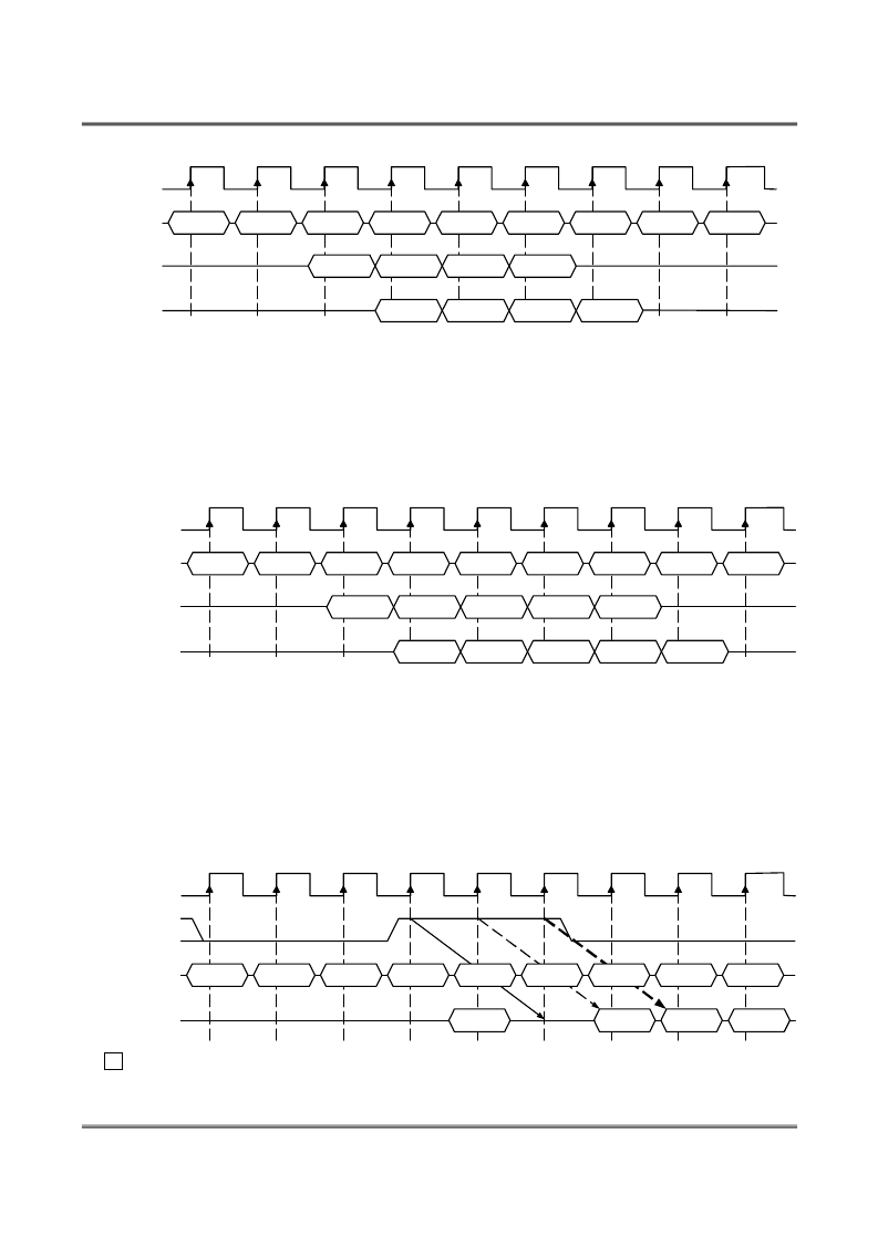
CLK
COMMAND
CAS# latency=2
tCK2, DQ's
CAS# latency=3
tCK3, DQ's
T0
T 1
T2
T3
T4
T5
T6
T7
T8
READ A
NOP
NOP
NOP
NOP
NOP
NOP
NOP
NOP
DOUT A0
DOUT A1
DOUT A2
DOUT A3
DOUT A0
DOUT A1
DOUT A2
DOUT A3
Burst Read Operation
(Burst Length = 4, CAS# Latency = 2, 3)
latency is two clocks for output buffers). A read burst without the auto precharge function may be interrupted
by a subsequent Read or Write command to the same bank or the other active bank before the end of the burst
length. It may be interrupted by a BankPrecharge/ PrechargeAll command to the same bank too. The interrupt
coming from the Read command can occur on any clock cycle following a previous Read command (refer to
the following figure).
The read data appears on the DQs subject to the values on the DQM inputs two clocks earlier (i.e. DQM
CLK
COMMAND
CAS# latency=2
tCK2, DQ's
CAS# latency=3
tCK3, DQ's
T0
T 1
T2
T3
T4
T5
T6
T7
T8
READ A
READ B
NOP
NOP
NOP
NOP
NOP
NOP
NOP
DOUT A0
DOUT B0
DOUT B1
DOUT B2
DOUT B3
DOUT A0
DOUT B0
DOUT B1
DOUT B2
DOUT B3
Read Interrupted by a Read
(Burst Length = 4, CAS# Latency = 2, 3)
command. The DQMs must be asserted (HIGH) at least two clocks prior to the Write command to suppress
data-out on the DQ pins. To guarantee the DQ pins against I/O contention, a single cycle with high-impedance
on the DQ pins must occur between the last read data and the Write command (refer to the following three
figures). If the data output of the burst read occurs at the second clock of the burst write, the DQMs must be
asserted (HIGH) at least one clock prior to the Write command to avoid internal bus contention.
The DQM inputs are used to avoid I/O contention on the DQ pins when the interrupt comes from a Write
READ A
NOP
NOP
NOP
NOP
WRITE B
NOP
NOP
CLK
DQM
COMMAND
DQ's
T0
T 1
T2
T3
T4
T5
T6
T7
T8
NOP
DOUT A0
DINB0
DINB1
DINB2
Must be Hi-Z before
the Write Command
: "H" or "L"
Read to Write Interval
(Burst Length
≥
4, CAS# Latency = 3)
相关PDF资料 |
PDF描述 |
|---|---|
| T436416D-6SG | 4M x 16 SDRAM 1M x 16bit x 4Banks Synchronous DRAM |
| T436416D-7C | 4M x 16 SDRAM 1M x 16bit x 4Banks Synchronous DRAM |
| T436416D-7CG | 4M x 16 SDRAM 1M x 16bit x 4Banks Synchronous DRAM |
| T436416D-7S | 4M x 16 SDRAM 1M x 16bit x 4Banks Synchronous DRAM |
| T436416D-7SG | 4M x 16 SDRAM 1M x 16bit x 4Banks Synchronous DRAM |
相关代理商/技术参数 |
参数描述 |
|---|---|
| T436416D-6SG | 制造商:TMT 制造商全称:TMT 功能描述:4M x 16 SDRAM 1M x 16bit x 4Banks Synchronous DRAM |
| T436416D-7C | 制造商:TMT 制造商全称:TMT 功能描述:4M x 16 SDRAM 1M x 16bit x 4Banks Synchronous DRAM |
| T436416D-7CG | 制造商:TMT 制造商全称:TMT 功能描述:4M x 16 SDRAM 1M x 16bit x 4Banks Synchronous DRAM |
| T436416D-7S | 制造商:TMT 制造商全称:TMT 功能描述:4M x 16 SDRAM 1M x 16bit x 4Banks Synchronous DRAM |
| T436416D-7SG | 制造商:TMT 制造商全称:TMT 功能描述:4M x 16 SDRAM 1M x 16bit x 4Banks Synchronous DRAM |
发布紧急采购,3分钟左右您将得到回复。