- 您现在的位置:买卖IC网 > PDF目录98158 > TAS3001CPW (TEXAS INSTRUMENTS INC) 2 CHANNEL(S), TONE CONTROL CIRCUIT, PDSO28 PDF资料下载
参数资料
| 型号: | TAS3001CPW |
| 厂商: | TEXAS INSTRUMENTS INC |
| 元件分类: | 音频控制 |
| 英文描述: | 2 CHANNEL(S), TONE CONTROL CIRCUIT, PDSO28 |
| 封装: | GREEN, PLASTIC, TSSOP-28 |
| 文件页数: | 13/55页 |
| 文件大小: | 432K |
| 代理商: | TAS3001CPW |
第1页第2页第3页第4页第5页第6页第7页第8页第9页第10页第11页第12页当前第13页第14页第15页第16页第17页第18页第19页第20页第21页第22页第23页第24页第25页第26页第27页第28页第29页第30页第31页第32页第33页第34页第35页第36页第37页第38页第39页第40页第41页第42页第43页第44页第45页第46页第47页第48页第49页第50页第51页第52页第53页第54页第55页
31
3 Serial Control Interface (I2C)
The TAS3001 operation is controlled using the RESET signal and the serial control interface. Control information is
downloaded into the TAS3001 control registers by an I2C master device, such as a microprocessor, microcontroller,
or DSP. These registers control the settings for volume, bass, treble, mixing, and filtering. A description of the register
addresses and control formats is given in Appendix A.
The I2C bus employs two signals, SDA (data) and SCL (clock), to communicate between integrated circuits in a
system. Each device is addressed by sending a unique 7-bit slave address plus an R/W bit (1 byte).
All I2C compatible devices are controlled using the SDA and SCL signals using a wire-ANDed connection. A pullup
resistor must be used to set the high level on the bus. The TAS3001 operates in standard I2C mode up to 100 kbps
with as many devices on the bus as desired up to the capacitance load limit of 400 pF.
The TAS3001 is an I2C slave-only device; therefore, at least one device connected to the I2C bus with this device
must operate in master mode. The pullup resistor is generally 4.99 k
. Upon power up, the I2C is in an unknown state
until the master clock has been applied and the TAS3001 has been reset. Prior to reset, the TAS3001 may hold the
SDA and/or SCL lines low. This creates I2C communication errors for any other device that attempts to use the bus.
3.1
I2C Protocol
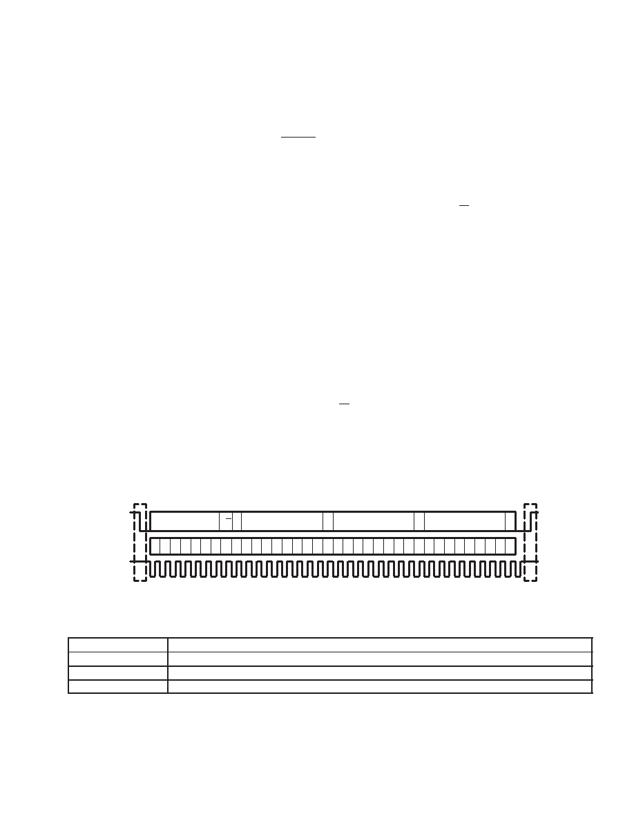
The bus standard uses transitions on the data pin (SDA) while the clock is high to indicate start and stop conditions.
A high-to-low transition on SDA indicates a start and a low-to-high transition indicates a stop. Normal data-bit
transitions must occur within the low time of the clock period. These conditions are shown in Figure 31. These start
and stop conditions for the I2C bus are required by standard protocol to be generated by the master. The master must
also generate the 7-bit slave address and the read/write (R/W) bit to open communication with another device and
then wait for an acknowledge condition. The slave holds SDA low during acknowledge clock period to indicate an
acknowledgment. When this occurs, the master transmits the next byte of the sequence.
After each 8-bit word, an acknowledgment must be transmitted by the receiving device. There is no limit on the
number of bytes that can be transmitted between start and stop conditions. When the last word transfers, the master
generates a stop condition to release the bus. A generic data transfer sequence is shown in Figure 31. Definitions
for the I2C protocol terms are listed in Table 31.
7 Bit Slave Address
R/W
8 Bit Subaddress (N)
AA
8 Bit Data For
Address (N)
A
8 Bit Data For
Address (N)
A
7
6
543
2
1
0
7
6
5
43
2
1
0
7
6
5
43
2
1
0
7
6
5
43
2
1
0
Start
Stop
SDA
SCL
Figure 31. Typical I2C Data Transfer Sequence
Table 31. I2C Protocol Definitions
DEFINITION
DESCRIPTION
Master
The device that initiates a transfer, generates clock signals, and terminates the transfer
Receiver
The device that receives data
Slave
The device addressed by the master
相关PDF资料 |
PDF描述 |
|---|---|
| TAS3002 | SPECIALTY CONSUMER CIRCUIT, PQFP48 |
| TAS3004PFB | SPECIALTY CONSUMER CIRCUIT, PQFP48 |
| TAS3004PFBR | SPECIALTY CONSUMER CIRCUIT, PQFP48 |
| TAS3004PFBG4 | SPECIALTY CONSUMER CIRCUIT, PQFP48 |
| TAS3004PFBRG4 | SPECIALTY CONSUMER CIRCUIT, PQFP48 |
相关代理商/技术参数 |
参数描述 |
|---|---|
| TAS3001CPWG4 | 功能描述:音频 DSP Stero Audio Digital Equalizer RoHS:否 制造商:Texas Instruments 工作电源电压: 电源电流: 工作温度范围: 安装风格: 封装 / 箱体: 封装:Tube |
| TAS3001CPWR | 功能描述:音频 DSP Stero Audio Digital Equalizer RoHS:否 制造商:Texas Instruments 工作电源电压: 电源电流: 工作温度范围: 安装风格: 封装 / 箱体: 封装:Tube |
| TAS3001CPWRG4 | 功能描述:音频 DSP Stero Audio Digital Equalizer RoHS:否 制造商:Texas Instruments 工作电源电压: 电源电流: 工作温度范围: 安装风格: 封装 / 箱体: 封装:Tube |
| TAS3001EVM | 制造商:Texas Instruments 功能描述:TAS3001 EVALUATION BOARD - Bulk |
| TAS3001IN WAF | 制造商:Texas Instruments 功能描述: |
发布紧急采购,3分钟左右您将得到回复。