参数资料
| 型号: | TBU-PL085-100-WH |
| 厂商: | Bourns Inc. |
| 文件页数: | 5/7页 |
| 文件大小: | 0K |
| 描述: | SURGE SUPP TBU DL 50OHM 850VIMP |
| 标准包装: | 1 |
| 系列: | TBU™ |
| 电压 - 工作: | 425V |
| 电压 - 箝位: | 850V |
| 技术: | 混合技术 |
| 电路数: | 2 |
| 应用: | SLIC |
| 封装/外壳: | SMD 6.50mm x 4.00mm |
| 供应商设备封装: | SMD |
| 包装: | 标准包装 |
| 其它名称: | TBU-PL085-100-WHDKR |
�� �
�
�TBU-PL� Series� -� TBU� ?� High-Speed� Protectors�
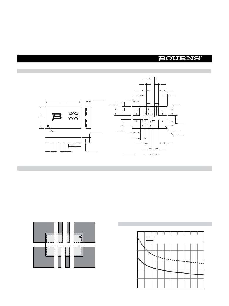
�Product� Dimensions�
�0.70�
�(.028)�
�0.825�
�(.032)�
�0.40�
�(.016)�
�0.825�
�(.032)�
�0.725�
�(.029)�
�1.275�
�(.050)�
�0.30�
�(.012)�
�6.50�
�(.256)�
�0.85� ±� 0.05�
�(.033� ±� .002)�
�1.335�
�0.30�
�(.012)�
�1.15�
�(.045)�
�1.20�
�(.047)�
�1.35�
�(.053)�
�1.275�
�(.053)�
�(.050)�
�0.73�
�(.029)�
�0.85�
�(.033)�
�0.85�
�(.033)�
�4.00�
�(.157)�
�1.335�
�1.35�
�(.053)�
�0.85�
�(.033)�
�1.20�
�(.047)�
�0.85�
�(.033)�
�1.275�
�(.010)�
�PIN� 1� &� BACKSIDE� CHAMFER�
�0.80� -� 0.95�
�(.031� -� .037)�
�(.053)�
�1.25�
�(.049)�
�0.75�
�(.050)�
�0.25�
�C� PIN� 1�
�0.90�
�(.030)�
�0.70�
�(.028)�
�1.30�
�(.051)�
�0.85�
�(.033)�
�0.85�
�(.033)�
�(.035)�
�0.00� -� 0.05�
�(.000� -� .002)�
�DIMENSIONS:�
�MM�
�(INCHES)�
�0.75�
�(.030)�
�0.40�
�(.016)�
�0.75�
�(.030)�
�Recommended� Pad� Layout�
�TBU� ?� High-Speed� Protectors� have� a� 100� %� matte-tin� termination�
�?nish.� For� improved� thermal� dissipation,� the� recommended� layout�
�uses� PCB� copper� areas� which� extend� beyond� the� exposed� solder�
�pad.� The� exposed� solder� pads� should� be� de?ned� by� a� solder� mask�
�which� matches� the� pad� layout� of� the� TBU� ?� device� in� size� and� spac-�
�ing.� It� is� recommended� that� they� should� be� the� same� dimension� as�
�the� TBU� ?� pads� but� if� smaller� solder� pads� are� used,� they� should� be�
�centered� on� the� TBU� ?� package� terminal� pads� and� not� more� than�
�0.10-0.12� mm� (0.004-0.005� in.)� smaller� in� overall� width� or� length.�
�Solder� pad� areas� should� not� be� larger� than� the� TBU� ?� pad� sizes�
�stencil� thickness� is� 0.10-0.12� mm� (0.004-0.005� in.)� with� a� stencil�
�opening� size� 0.025� mm� (0.0010� in.)� less� than� the� solder� pad�
�size.� Extended� copper� areas� beyond� the� solder� pad� signi?cantly�
�improve� the� junction� to� ambient� thermal� resistance,� resulting� in�
�operation� at� lower� junction� temperatures� with� a� corresponding�
�bene?t� of� reliability.� All� pads� should� soldered� to� the� PCB,� includ-�
�ing� pads� marked� as� NC� or� NU� but� no� electrical� connection� should�
�be� made� to� these� pads.� For� minimum� parasitic� capacitance,� it� is�
�recommended� that� signal,� ground� or� power� signals� are� not� routed�
�beneath� any� pad.�
�to� ensure� adequate� clearance� is� maintained.� The� recommended�
�Thermal� Resistance� vs� Additional� PCB� Cu� Area�
�120�
�4�
�5�
�3�
�6�
�2�
�7�
�1�
�8�
�100�
�80�
�Power� in� One� Side� of� TBU� ?� Device�
�Total� Power� in� Both� Sides� of� TBU� ?� Device�
�60�
�40�
�Dark� grey� areas� show� added� PCB� copper� area� for� better�
�thermal� resistance.�
�20�
�0�
�Speci?cations� are� subject� to� change� without� notice.�
�0�
�0.2�
�0.4�
�0.6�
�0.8�
�1.0�
�1.2�
�1.4�
�1.6�
�1.8�
�2.0�
�Customers� should� verify� actual� device� performance� in� their� speci?c� applications.�
�Added� Cu� Area� (Sq.� In.)�
�相关PDF资料 |
PDF描述 |
|---|---|
| TC2030-MCP-NL | CABLE TAG-CONNECT IN-CIRCUIT |
| TC2030-MCP | CABLE TAG-CONNECT IN-CIRCUIT LEG |
| TC2050-IDC-430 | CBL PLUG-OF-NAILS MSP430 LEG TI |
| TC2050-IDC-NL-430 | CBL PLUG-OF-NAILS MSP430 TI |
| TC2050-IDC-NL | CBL PLUG-OF-NAILS 10-PIN |
相关代理商/技术参数 |
参数描述 |
|---|---|
| TBU-PL085-100-WH | 制造商:Bourns Inc 功能描述:Transient Blocking Unit |
| TBU-PL085-200-WH | 功能描述:浪涌抑制器 Dual 50ohm TBU Devce Bi-directional RoHS:否 制造商:Bourns 电压额定值:40 V 电流额定值:750 mA 工作温度范围:- 40 C to + 125 C 端接类型:SMD/SMT 封装 / 箱体: |
| TBU-PL085-200-WH | 制造商:Bourns Inc 功能描述:Transient Blocking Unit |
| TBV-100M-2A-3026 | 制造商:SUPERWORLD 制造商全称:Superworld Electronics 功能描述:TOROIDAL INDUCTOR |
| TBV-101M-2A-5026 | 制造商:SUPERWORLD 制造商全称:Superworld Electronics 功能描述:TOROIDAL INDUCTOR |
发布紧急采购,3分钟左右您将得到回复。