- 您现在的位置:买卖IC网 > PDF目录220057 > TC1219ECHRT 0.05 A SWITCHED CAPACITOR CONVERTER, 20 kHz SWITCHING FREQ-MAX, PDSO6 PDF资料下载
参数资料
| 型号: | TC1219ECHRT |
| 元件分类: | 稳压器 |
| 英文描述: | 0.05 A SWITCHED CAPACITOR CONVERTER, 20 kHz SWITCHING FREQ-MAX, PDSO6 |
| 封装: | SOT-23A, 6 PIN |
| 文件页数: | 2/8页 |
| 文件大小: | 85K |
| 代理商: | TC1219ECHRT |
2
TC1219/1220-3 8/20/99
SWITCHED CAPACITOR VOLTAGE
CONVERTERS WITH SHUTDOWN
IN SOT PACKAGES
TC1219
TC1220
ABSOLUTE MAXIMUM RATINGS*
Input Voltage (VIN to GND) ......................... +6.0V, – 0.3V
Output Voltage (OUT to GND) .................... –6.0V, + 0.3V
Current at OUT Pin ................................................. 50 mA
Short-Circuit Duration – OUT to GND ................ Indefinite
Operating Temperature Range ............... – 40
°C to +85°C
Power Dissipation (TA ≤ 70°C)
6-Pin SOT-23A .............................................. 240 mW
Storage Temperature (Unbiased) ......... – 65
°C to +150°C
Lead Temperature (Soldering, 10 sec) ................. +260
°C
*This is a stress rating only and functional operation of the device at these
or any other conditions above those indicated in the operational sections
of the specifications is not implied. Exposure to absolute maximum rating
conditions for extended periods may affect device reliability.
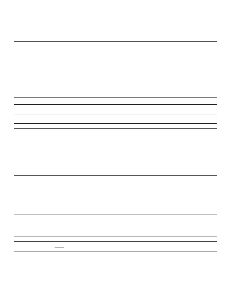
ELECTRICAL CHARACTERISTICS: TA = –40°C to +85°C, VIN = +5V, C1 = C2 = 10 F (TC1219), C1 = C2 = 3.3F
(TC1220), unless otherwise noted. Typical values are at TA = +25°C.
Symbol Parameter
Device
Test Conditions
Min
Typ
Max
Unit
IDD
Supply Current
TC1219
—
60
115
A
TC1220
—
115
325
ISHDN
Shutdown Supply Current
SHDN = GND,
—
0.1
1.0
A
VIN = 5V (Note 2)
VMIN
Minimum Supply Voltage
RLOAD = 1 K
2.5
—
V
VMAX
Maximum Supply Voltage
RLOAD = 1 K
—
5.5
V
FOSC
Oscillator Frequency
TC1219
6
12
20
KHz
TC1220
19
35
56.3
VIH
Shutdown Input
RLOAD = ∞
Logic High
TC1219
VIN = VMIN to 3V
1.5
—
V
VIN = >3V to VMAX
1.8
—
V
TC1220
VIN = VMIN to VMAX
1.5
—
V
VIL
Shutdown Input Logic Low
VIN = VMIN to VMAX
—
0.5
V
PEFF
Power Efficiency
TC1219
RLOAD = 1 K
—96
—
%
TC1220
95
VEFF
Voltage Conversion
RLOAD = ∞
95
99.9
—
%
Efficiency
ROUT
Output Resistance
TC1219/20
ILOAD = 0.5mA to 25mA
—
25
65
(Note 1)
NOTES: 1. Capacitor contribution is approximately 20% of the output impedance [ESR = 1 / pump frequency x capacitance)].
2. VIN is guaranteed to be disconnected from OUT when the converter is in shutdown.
PIN DESCRIPTION
Pin No.
(6-Pin SOT-23A)
Symbol
Description
1
OUT
Inverting Charge Pump Output.
2VIN
Positive Power Supply Input.
3C
–
Commutation Capacitor Negative Terminal.
4
GND
Ground.
5
SHDN
Shutdown Input (Active Low).
6C
+
Commutation Capacitor Positive Terminal.
相关PDF资料 |
PDF描述 |
|---|---|
| TC1121EOA723 | SWITCHED CAPACITOR CONVERTER, 200 kHz SWITCHING FREQ-MAX, PDSO8 |
| TPS2310IPWR | 2-CHANNEL POWER SUPPLY SUPPORT CKT, PDSO20 |
| TC6502P095VCT | SPECIALTY ANALOG CIRCUIT, PDSO5 |
| TPB-5/5-15/1-Q12 | 3-OUTPUT 25 W DC-DC REG PWR SUPPLY MODULE |
| TL4051CQDBZRG4 | 1-OUTPUT TWO TERM VOLTAGE REFERENCE, 1.212 V, PDSO3 |
相关代理商/技术参数 |
参数描述 |
|---|---|
| TC1219ECHTR | 功能描述:电荷泵 Switched CAP RoHS:否 制造商:Maxim Integrated 功能:Inverting, Step Up 输出电压:- 1.5 V to - 5.5 V, 3 V to 11 V 输出电流:100 mA 电源电流:1 mA 最大工作温度:+ 70 C 封装 / 箱体:SOIC-8 Narrow 封装:Tube |
| TC121A | 制造商:Thomas & Betts 功能描述:Fittings Connector 0.5inch Steel |
| TC121A-FA | 制造商:Thomas & Betts 功能描述:Fittings Connector 0.5inch Steel |
| TC121SC-50CP | 制造商:Thomas & Betts 功能描述:1/2" SET SCREW CONNECTOR 制造商:Thomas & Betts 功能描述:ADVANTAGES OF STEEL CITY COMMERCIAL CONDUIT FITTINGS |
| TC121TB | 制造商:Thomas & Betts 功能描述:Cable Accessories Snap In Mounting Base Cap Nylon 6.6 Natural Bulk |
发布紧急采购,3分钟左右您将得到回复。