- 您现在的位置:买卖IC网 > PDF目录220057 > TC1219ECHRT 0.05 A SWITCHED CAPACITOR CONVERTER, 20 kHz SWITCHING FREQ-MAX, PDSO6 PDF资料下载
参数资料
| 型号: | TC1219ECHRT |
| 元件分类: | 稳压器 |
| 英文描述: | 0.05 A SWITCHED CAPACITOR CONVERTER, 20 kHz SWITCHING FREQ-MAX, PDSO6 |
| 封装: | SOT-23A, 6 PIN |
| 文件页数: | 3/8页 |
| 文件大小: | 85K |
| 代理商: | TC1219ECHRT |
3
TC1219/1220-3 8/20/99
TC1219
TC1220
SWITCHED CAPACITOR VOLTAGE
CONVERTERSWITH SHUTDOWN
IN SOT PACKAGES
DETAILED DESCRIPTION
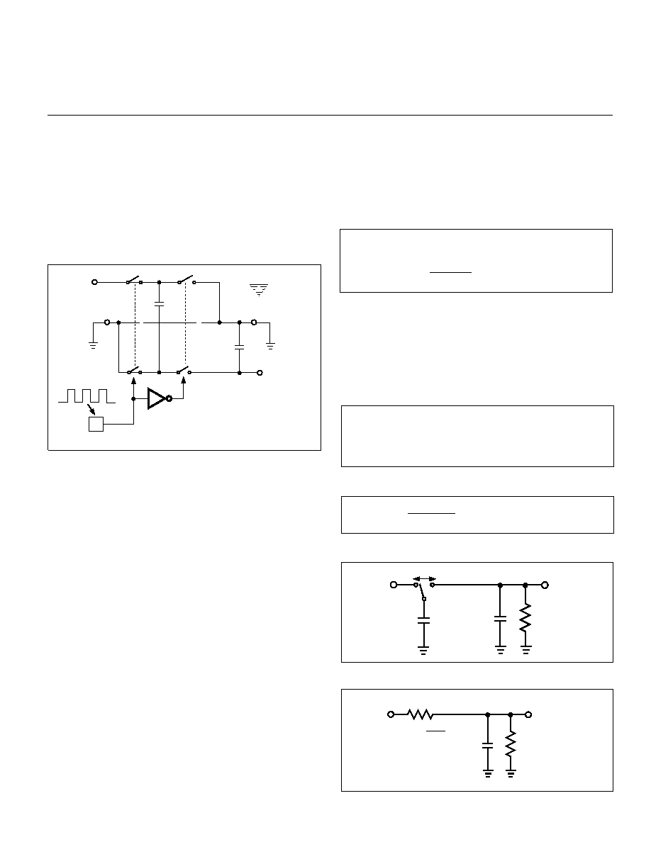
The TC1219/1220 charge pump converters invert the
voltage applied to the VIN pin. Conversion consists of a two-
phase operation (Figure 1). During the first phase, switches
S2 and S4 are opened and S1 and S3 are closed. During this
time, C1 charges to the voltage on VIN and load current is
supplied from C2. During the second phase, S2 and S4 are
closed, and S1 and S3 are opened. This action connects C1
across C2, restoring charge to C2.
APPLICATIONS INFORMATION
Output Voltage Considerations
The TC1219/1220 perform voltage conversion but do
not provide
regulation. The output voltage will droop in a
linear manner with respect to load current. The value of this
equivalent output resistance is approximately 25
nominal
at +25
°C and VIN = +5V. VOUT is approximately – 5V at light
loads, and droops according to the equation below:
VDROP = IOUT x ROUT
VOUT = – (VIN – VDROP)
Charge Pump Efficiency
The overall power efficiency of the charge pump is
affected by four factors:
(1) Losses from power consumed by the internal oscil-
lator, switch drive, etc. (which vary with input volt-
age, temperature and oscillator frequency).
(2) I
2R losses due to the on-resistance of the MOSFET
switches on-board the charge pump.
(3) Charge pump capacitor losses due to effective
series resistance (ESR).
Figure 1. Ideal Switched Capacitor Charge Pump
(4) Losses that occur during charge transfer (from the
commutation capacitor to the output capacitor)
when a voltage difference between the two capaci-
tors exists.
Most of the conversion losses are due to factors (2) and
(3) above. These losses are given by Equation 1(b).
(a) PLOSS (2, 3) = IOUT
2 x ROUT
(b) Where ROUT =
[ 1 +8RSWITCH+4ESRC1+ESRC2]
(fOSC)(C1)
The 1/(fOSC)(C1) term in Equation 1(b) is the effective
output resistance of an ideal switched capacitor circuit
(Figures 2a, 2b). The value of RSWITCH can be approximated
at 0.5
for the TC1219/1220.
The remaining losses in the circuit are due to factor
(4) above, and are shown in Equation 2. The output voltage
ripple is given by Equation 3.
PLOSS(4)=
[(0.5)(C1)(V
IN
2– V
OUT
2) + (0.5)(C2)(V
RIPPLE
2
– 2VOUTVRIPPLE)
] x fOSC
VRIPPLE =
IOUT
+2(IOUT)(ESRC2)
(fOSC)(C2)
Equation 2.
VOUT = – (VIN)
C1
C2
TC1219/1220
Phase 1
VIN
S1
S3
S4
S2
OSC
Equation 1.
Equation 3.
Figure 2a. Ideal Switched Capacitor Model
Figure 2b. Equivalent Output Resistance
V+
V
OUT
R
L
C1
C2
f
V+
V
OUT
R
EQUIV
R
EQUIV =
R
L
C2
f x C1
1
相关PDF资料 |
PDF描述 |
|---|---|
| TC1121EOA723 | SWITCHED CAPACITOR CONVERTER, 200 kHz SWITCHING FREQ-MAX, PDSO8 |
| TPS2310IPWR | 2-CHANNEL POWER SUPPLY SUPPORT CKT, PDSO20 |
| TC6502P095VCT | SPECIALTY ANALOG CIRCUIT, PDSO5 |
| TPB-5/5-15/1-Q12 | 3-OUTPUT 25 W DC-DC REG PWR SUPPLY MODULE |
| TL4051CQDBZRG4 | 1-OUTPUT TWO TERM VOLTAGE REFERENCE, 1.212 V, PDSO3 |
相关代理商/技术参数 |
参数描述 |
|---|---|
| TC1219ECHTR | 功能描述:电荷泵 Switched CAP RoHS:否 制造商:Maxim Integrated 功能:Inverting, Step Up 输出电压:- 1.5 V to - 5.5 V, 3 V to 11 V 输出电流:100 mA 电源电流:1 mA 最大工作温度:+ 70 C 封装 / 箱体:SOIC-8 Narrow 封装:Tube |
| TC121A | 制造商:Thomas & Betts 功能描述:Fittings Connector 0.5inch Steel |
| TC121A-FA | 制造商:Thomas & Betts 功能描述:Fittings Connector 0.5inch Steel |
| TC121SC-50CP | 制造商:Thomas & Betts 功能描述:1/2" SET SCREW CONNECTOR 制造商:Thomas & Betts 功能描述:ADVANTAGES OF STEEL CITY COMMERCIAL CONDUIT FITTINGS |
| TC121TB | 制造商:Thomas & Betts 功能描述:Cable Accessories Snap In Mounting Base Cap Nylon 6.6 Natural Bulk |
发布紧急采购,3分钟左右您将得到回复。