- 您现在的位置:买卖IC网 > PDF目录98183 > TC850ILW 1-CH 15-BIT MULTI-SLOPE ADC, PARALLEL ACCESS, PQCC44 PDF资料下载
参数资料
| 型号: | TC850ILW |
| 元件分类: | ADC |
| 英文描述: | 1-CH 15-BIT MULTI-SLOPE ADC, PARALLEL ACCESS, PQCC44 |
| 封装: | PLASTIC, LCC-44 |
| 文件页数: | 23/26页 |
| 文件大小: | 417K |
| 代理商: | TC850ILW |
TC850
DS21479C-page 6
2006 Microchip Technology Inc.
2.0
PIN DESCRIPTIONS
The descriptions of the pins are listed in Table .
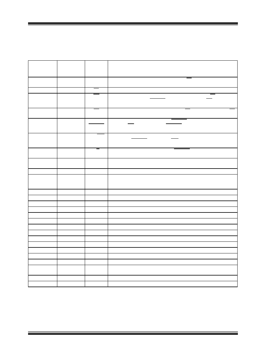
TABLE 2-1:
PIN FUNCTION TABLE
Pin Number
(40-Pin
PDIP/CERDIP)
Pin Number
(44-Pin PLCC)
Symbol
Description
1
2
CS
Chip Select, active HIGH. Logically ANDed, with CE to enable read and write
inputs (Note 1).
23
CE
Chip enable, active LOW (Note 2).
34
WR
Write input, active LOW. When chip is selected (CS = HIGH and CE = LOW) and
in Demand mode (CONT/DEMAND = LOW), a logic LOW on WR starts a
conversion (Note 1).
45
RD
Read input, active LOW. When CS = HIGH and CE = LOW, a logic LOW on RD
enables the 3-state data outputs (Note 2).
5
6
CONT/
DEMAND
Conversion control input. When CONT/DEMAND = LOW, conversions are initi-
ated by the WR input. When CONT/DEMAND = HIGH, conversions are
performed continuously (Note 1).
67
OVR/POL
Overrange/polarity data-select input. When making conversions in the Demand
mode (CONT/DEMAND = LOW), OVR/POL controls the data output on DB7
when the high-order byte is active (Note 2).
78
L/H
Low/high byte-select input. When CONT/DEMAND = LOW, this input controls
whether low-byte or high-byte data is enabled on DB0 through DB7 (Note 2).
8
9
DB7
Most Significant data bit output. When reading the A/D conversion result, the
polarity, overrange and DB7 data are output on this pin.
9-15
10-17
DB6-DB0
Data outputs DB6-DB0. 3-state, bus compatible.
16
18
BUSY
A/D conversion status output. BUSY goes to a logic HIGH at the beginning of the
de-integrate phase, then goes LOW when conversion is complete. The falling
edge of BUSY can be used to generate a
μP interrupt.
17
19
OSC1
Crystal oscillator connection or external oscillator input.
18
20
OSC2
Crystal oscillator connection.
19
21
TEST
For factory testing purposes only. Do not make external connection to this pin.
20
22
DGND
Digital ground connection.
21
24
COMP
Connection for comparator auto-zero capacitor. Bypass to VSS with 0.1 μF.
22
25
VSS
Negative power supply connection, typically -5V.
23
26
INTOUT
Output of the integrator amplifier. Connect to CINT.
24
27
INTIN
Input to the integrator amplifier. Connect to summing node of RINT and CINT.
25
28
BUFFER
Output of the input buffer. Connect to RINT.
26
29
CBUFB
Connection for buffer auto-zero capacitor. Bypass to VSS with 0.1 μF.
27
30
CBUFA
Connection to buffer auto-zero capacitor. Bypass to VSS with 0.1 μF.
28
31
CINTA
Connection for integrator auto-zero capacitor. Bypass to VSS with 0.1 μF.
29
32
CINTB
Connection for integrator auto-zero capacitor. Bypass to VSS with 0.1 μF.
30
33
ANALOG
COMMON
Analog common.
31
35
IN–
Negative differential analog input.
32
36
IN+
Positive differential analog input.
Note
1:
This pin incorporates a pull-down resistor to DGND.
2: This pin incorporates a pull-up resistor to VDD.
3: Pins 1, 23 and 34 (44-PLCC) package are NC “No Internal connection”.
相关PDF资料 |
PDF描述 |
|---|---|
| TC9028P | INFRARED, TRANSMITTER IC, PDIP20 |
| TC9028F | INFRARED, TRANSMITTER IC, PDSO20 |
| TC9083N | PICTURE-IN-PICTURE IC, PDIP42 |
| TC9090AN | Y/C SEPARATOR IC, PDIP28 |
| TC9090AF | Y/C SEPARATOR IC, PDSO28 |
相关代理商/技术参数 |
参数描述 |
|---|---|
| TC850ILW713 | 功能描述:模数转换器 - ADC 16 Bit Hi Speed A/D RoHS:否 制造商:Texas Instruments 通道数量:2 结构:Sigma-Delta 转换速率:125 SPs to 8 KSPs 分辨率:24 bit 输入类型:Differential 信噪比:107 dB 接口类型:SPI 工作电源电压:1.7 V to 3.6 V, 2.7 V to 5.25 V 最大工作温度:+ 85 C 安装风格:SMD/SMT 封装 / 箱体:VQFN-32 |
| TC8521AM | 制造商:TOSHIBA 制造商全称:Toshiba Semiconductor 功能描述:REAL TIME CLOCK ケ |
| TC8521AP | 制造商:TOSHIBA 制造商全称:Toshiba Semiconductor 功能描述:REAL TIME CLOCK ケ |
| TC8566AF | 制造商:TOSHIBA 制造商全称:Toshiba Semiconductor 功能描述:FLOPPY DISK CONTROLLER |
| TC8569AF | 制造商:TOSHIBA 制造商全称:Toshiba Semiconductor 功能描述:FLOPPY DISK CONTROLLER |
发布紧急采购,3分钟左右您将得到回复。