- 您现在的位置:买卖IC网 > PDF目录98211 > TEA5766UK/N1/S21,1 (NXP SEMICONDUCTORS) FM, AUDIO SINGLE CHIP RECEIVER, PBGA25 PDF资料下载
参数资料
| 型号: | TEA5766UK/N1/S21,1 |
| 厂商: | NXP SEMICONDUCTORS |
| 元件分类: | 接收器 |
| 英文描述: | FM, AUDIO SINGLE CHIP RECEIVER, PBGA25 |
| 封装: | 3.30 X 3.25 MM, 0.60 MM HEIGHT, WLCSP-25 |
| 文件页数: | 27/59页 |
| 文件大小: | 273K |
| 代理商: | TEA5766UK/N1/S21,1 |
第1页第2页第3页第4页第5页第6页第7页第8页第9页第10页第11页第12页第13页第14页第15页第16页第17页第18页第19页第20页第21页第22页第23页第24页第25页第26页当前第27页第28页第29页第30页第31页第32页第33页第34页第35页第36页第37页第38页第39页第40页第41页第42页第43页第44页第45页第46页第47页第48页第49页第50页第51页第52页第53页第54页第55页第56页第57页第58页第59页
TEA5766UK_1
NXP B.V. 2007. All rights reserved.
Product data sheet
Rev. 01 — 22 March 2007
33 of 59
NXP Semiconductors
TEA5766UK
Stereo FM radio + RDS
[1]
The maximum fall time for the SDA and SCL bus lines quoted in table 5 of Ref. 1, 300 ns, is shorter than the specied maximum for the
output stages, 350 ns, therefore no series protection resistors may be connected between the SDA and SCL pins and the SDA and SCL
bus lines as shown in gure 36 of Ref. 1.
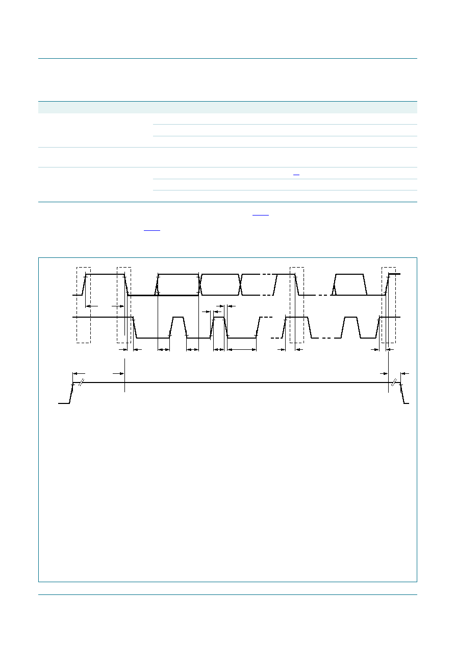
10.2.3 I2C-bus timing diagram
Table 10.
Characteristics of the data output stage for fast mode and standard mode
Symbol
Parameter
Conditions
Min
Typ
Max
Unit
VOL1
LOW-level output
voltage
open collector; Isink = 2 mA; VVREFDIG >2V
standard mode
0
-
0.5
V
fast mode
0
-
0.5
V
VOL3
LOW-level output
voltage
fast mode; open collector; Isink = 2 mA;
VVREFDIG <2V
0
-
0.5
V
tof
output fall time
standard mode
250
-
350
ns
fast mode
250
-
350
ns
In TEA5766UK, signal SDA is present on pin DATA and signal SCL on pin CLOCK.
Cb = capacitive load for each bus line: < 100 pF.
tf = fall time of both SDA and SCL signals: 20 + 0.1 Cb < tf < 350 ns, where Cb = total capacitance on bus line in pF.
tr = rise time of both SDA and SCL signals: 20 + 0.1 Cb < tf < 350 ns, where Cb = total capacitance on bus line in pF.
tHD;STA = hold time (repeated) START condition. After this period, the rst clock pulse is generated: > 600 ns.
tHIGH = HIGH period of the SCL clock: > 600 ns.
tLOW = LOW period of the SCL clock: > 1.3 s
tSU;STA = set-up time for a repeated START condition: > 600 ns.
tHD;DAT = data hold time: 300 ns < tHD;DAT < 900 ns.
Remark: 300 ns lower limit is added because the TEA5766UK has no internal hold time for the SDA signal.
tSU;DAT = data set-up time: > 100 ns. If TEA5766UK is used in a standard mode I2C-bus system, tSU;DAT > 250 ns.
tSU;STO = set-up time for STOP condition: > 600 ns.
tBUF = bus free time between a STOP and a START condition: > 600 ns.
tsu(BUSEN) = set-up time on pin BUSEN (bus enable): > 10 s.
th(BUSEN) = hold time on pin BUSEN: > 10 s.
Fig 16. I2C-bus timing diagram
P
S
Sr
P
001aaf518
tHD;STA
tBUF
tSU;STA
tSU;DAT
tf
tHIGH
tLOW
tSU;STO
tr
tHD;DAT
SDA
SCL
BUSEN
tsu(BUSEN)
th(BUSEN)
相关PDF资料 |
PDF描述 |
|---|---|
| TEA5766UK | FM, AUDIO SINGLE CHIP RECEIVER, PBGA25 |
| TEA5777HL/N2,118 | AM/FM, AUDIO SINGLE CHIP RECEIVER, PQFP32 |
| TEA5777HN/N2,518 | AM/FM, AUDIO SINGLE CHIP RECEIVER, PQCC48 |
| TEA6300PN | 2 CHANNEL(S), SOUND FADER CONTROL CIRCUIT, PDIP28 |
| TEA6300TD-T | 2 CHANNEL(S), SOUND FADER CONTROL CIRCUIT, PDSO28 |
相关代理商/技术参数 |
参数描述 |
|---|---|
| TEA5767 | 制造商:PHILIPS 制造商全称:NXP Semiconductors 功能描述:single-chip FM stereo radio |
| TEA5767HL | 制造商:PHILIPS 制造商全称:NXP Semiconductors 功能描述:Low-power FM stereo radio for handheld applications |
| TEA5767HN | 制造商:PHILIPS 制造商全称:NXP Semiconductors 功能描述:Low-power FM stereo radio for handheld applications |
| TEA5767HN/V3 | 功能描述:射频收发器 FM RECEIVER RoHS:否 制造商:Atmel 频率范围:2322 MHz to 2527 MHz 最大数据速率:2000 Kbps 调制格式:OQPSK 输出功率:4 dBm 类型: 工作电源电压:1.8 V to 3.6 V 最大工作温度:+ 85 C 接口类型:SPI 封装 / 箱体:QFN-32 封装:Tray |
| TEA5767HN/V3,118 | 功能描述:射频收发器 FM RECEIVER RoHS:否 制造商:Atmel 频率范围:2322 MHz to 2527 MHz 最大数据速率:2000 Kbps 调制格式:OQPSK 输出功率:4 dBm 类型: 工作电源电压:1.8 V to 3.6 V 最大工作温度:+ 85 C 接口类型:SPI 封装 / 箱体:QFN-32 封装:Tray |
发布紧急采购,3分钟左右您将得到回复。