- 您现在的位置:买卖IC网 > PDF目录69485 > THMC40DR (TEXAS INSTRUMENTS INC) BRUSHLESS DC MOTOR CONTROLLER, 1.5 A, PDSO14 PDF资料下载
参数资料
| 型号: | THMC40DR |
| 厂商: | TEXAS INSTRUMENTS INC |
| 元件分类: | 运动控制电子 |
| 英文描述: | BRUSHLESS DC MOTOR CONTROLLER, 1.5 A, PDSO14 |
| 封装: | PLASTIC, SOP-14 |
| 文件页数: | 13/19页 |
| 文件大小: | 300K |
| 代理商: | THMC40DR |
THMC40, THMC41
VARIABLE SPEED 12-VDC BRUSHLESS FAN MOTOR DRIVERS
SLIS097 – MARCH 2000
3
POST OFFICE BOX 655303
DALLAS, TEXAS 75265
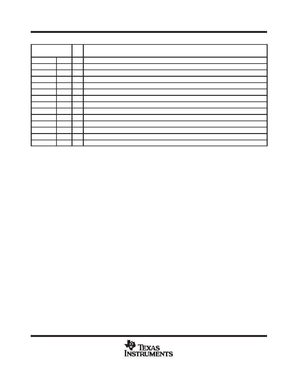
Terminal Functions
TERMINAL
I/O
DESCRIPTION
NAME
NO.
I/O
DESCRIPTION
AGND
9
I
IC analog ground and substrate connection
CP
3
I
External charge pump capacitor
COSC
1
I/O
External oscillator capacitor
H–
12
I
Hall sensor negative input
H+
13
I
Hall sensor positive input
NC
6, 8
–
No connection
PGND
7
I
Power ground for high-side charge pump
PHA
11
O
Low-side driver for phase A motor winding
PHB
10
O
Low-side driver for phase B motor winding
RD
2
O
Open-drain locked rotor detection output—THMC41 only
TACH
2
O
Open-drain tachometer output signal—THMC40 only
VOUT
5
O
High-side PWM driver output for motor windings
VPWR
4
I
Supply voltage input
VPWM
14
I
PWM duty cycle control voltage input
absolute maximum ratings over operating case temperature range (unless otherwise noted)
(see Note 1)
Supply voltage input, VPWR
18 V
. . . . . . . . . . . . . . . . . . . . . . . . . . . . . . . . . . . . . . . . . . . . . . . . . . . . . . . . . . . . . . . . .
High-side driver, PWM output voltage, VOUT
18 V
. . . . . . . . . . . . . . . . . . . . . . . . . . . . . . . . . . . . . . . . . . . . . . . . . .
Low-side drivers, phase A and B output, VPHA, VPHB
40 V
. . . . . . . . . . . . . . . . . . . . . . . . . . . . . . . . . . . . . . . . . .
Hall sensor amplifier input voltage, VH+, VH–
7 V
. . . . . . . . . . . . . . . . . . . . . . . . . . . . . . . . . . . . . . . . . . . . . . . . . . .
PWM duty cycle control input voltage, VPWM
7 V
. . . . . . . . . . . . . . . . . . . . . . . . . . . . . . . . . . . . . . . . . . . . . . . . . . .
Open-drain tachometer output voltage (THMC40), VTACH, or open-drain RD output voltage
(THMC41), VRD
7 V
. . . . . . . . . . . . . . . . . . . . . . . . . . . . . . . . . . . . . . . . . . . . . . . . . . . . . . . . . . . . . . . . . . . . . . . . .
Oscillator capacitor voltage, VCOSC
7 V
. . . . . . . . . . . . . . . . . . . . . . . . . . . . . . . . . . . . . . . . . . . . . . . . . . . . . . . . . . .
Charge pump capacitor voltage, VCP
30 V
. . . . . . . . . . . . . . . . . . . . . . . . . . . . . . . . . . . . . . . . . . . . . . . . . . . . . . . . .
Continuous high-side PWM output source/sink current, IOUT
1.5 A
. . . . . . . . . . . . . . . . . . . . . . . . . . . . . . . . . . .
Continuous low-side PWM output sink current, IPHA, IPHB
1.5 A
. . . . . . . . . . . . . . . . . . . . . . . . . . . . . . . . . . . . .
Junction-to-case thermal resistance, RθJC
26.9
°C/W
. . . . . . . . . . . . . . . . . . . . . . . . . . . . . . . . . . . . . . . . . . . . . . .
Junction-to-ambient thermal resistance , RθJA (see Note 2)
122.3
°C/W
. . . . . . . . . . . . . . . . . . . . . . . . . . . . . . .
Continuous power dissipation at 25
°C , PD (see Note 3)
1022 mW
. . . . . . . . . . . . . . . . . . . . . . . . . . . . . . . . . . .
Power derating factor above 25
°C ambient , PDERATING (see Note 4)
8.18 mW/
°C
. . . . . . . . . . . . . . . . . . . . .
Operating case temperature range, TC
–30
°C to 80°C
. . . . . . . . . . . . . . . . . . . . . . . . . . . . . . . . . . . . . . . . . . . . . .
Storage temperature range, Tstg
–55
°C to 150°C
. . . . . . . . . . . . . . . . . . . . . . . . . . . . . . . . . . . . . . . . . . . . . . . . . . .
Maximum junction temperature, TJ
150
°C
. . . . . . . . . . . . . . . . . . . . . . . . . . . . . . . . . . . . . . . . . . . . . . . . . . . . . . . . .
Lead temperature (soldering, 10 sec), TLEAD
300
°C
. . . . . . . . . . . . . . . . . . . . . . . . . . . . . . . . . . . . . . . . . . . . . . . .
Stresses beyond those listed under “absolute maximum ratings” may cause permanent damage to the device. These are stress ratings only, and
functional operation of the device at these or any other conditions beyond those indicated under “recommended operating conditions” is not
implied. Exposure to absolute-maximum-rated conditions for extended periods may affect device reliability.
NOTES:
1. All voltage values are with respect to GND.
2. JEDEC low-K board with 0 LFM airflow
3. 150
°C maximum junction temperature, JEDEC low-K board with 0 LFM airflow
4. 80
°C maximum ambient and 150°C maximum junction temperature
相关PDF资料 |
PDF描述 |
|---|---|
| THMC45DGNR | BRUSHLESS DC MOTOR CONTROLLER, PDSO8 |
| THS7002CPWP | SPECIALTY ANALOG CIRCUIT, PDSO28 |
| THS7002IPWP | SPECIALTY ANALOG CIRCUIT, PDSO28 |
| THS7001IPWP | SPECIALTY ANALOG CIRCUIT, PDSO20 |
| TIL5942ANFC | 2 A SWITCHING CONTROLLER, 1000 kHz SWITCHING FREQ-MAX, PDIP16 |
相关代理商/技术参数 |
参数描述 |
|---|---|
| THMC40SOPD | 制造商:TI 制造商全称:Texas Instruments 功能描述:VARIABLE SPEED 12-VDC BRUSHLESS FAN MOTOR DRIVERS |
| THMC41 | 制造商:TI 制造商全称:Texas Instruments 功能描述:VARIABLE SPEED 12-VDC BRUSHLESS FAN MOTOR DRIVERS |
| THMC41SOPD | 制造商:TI 制造商全称:Texas Instruments 功能描述:VARIABLE SPEED 12-VDC BRUSHLESS FAN MOTOR DRIVERS |
| THMC45 | 制造商:TI 制造商全称:Texas Instruments 功能描述:5-V AND 3.3-V DC BRUSHLESS FAN MOTOR DRIVER WITH SINGLE WIRE CONTOL |
| THMC50 | 制造商:TI 制造商全称:Texas Instruments 功能描述:REMOTE/LOCAL TEMPERATURE MONITOR AND FAN CONTROLLER WITH SMBus INTERFACE |
发布紧急采购,3分钟左右您将得到回复。