参数资料
| 型号: | THS4031IDGNG4 |
| 厂商: | Texas Instruments |
| 文件页数: | 21/47页 |
| 文件大小: | 0K |
| 描述: | IC OPAMP VFB 100MHZ SGL 8MSOP |
| 标准包装: | 80 |
| 放大器类型: | 电压反馈 |
| 电路数: | 1 |
| 转换速率: | 100 V/µs |
| -3db带宽: | 100MHz |
| 电流 - 输入偏压: | 3µA |
| 电压 - 输入偏移: | 500µV |
| 电流 - 电源: | 8.5mA |
| 电流 - 输出 / 通道: | 90mA |
| 电压 - 电源,单路/双路(±): | 9 V ~ 32 V,±4.5 V ~ 16 V |
| 工作温度: | -40°C ~ 85°C |
| 安装类型: | 表面贴装 |
| 封装/外壳: | 8-TSSOP,8-MSOP(0.118",3.00mm 宽)裸露焊盘 |
| 供应商设备封装: | 8-MSOP-PowerPad |
| 包装: | 管件 |
| 配用: | 296-10029-ND - EVAL MOD FOR THS4031 |
第1页第2页第3页第4页第5页第6页第7页第8页第9页第10页第11页第12页第13页第14页第15页第16页第17页第18页第19页第20页当前第21页第22页第23页第24页第25页第26页第27页第28页第29页第30页第31页第32页第33页第34页第35页第36页第37页第38页第39页第40页第41页第42页第43页第44页第45页第46页第47页
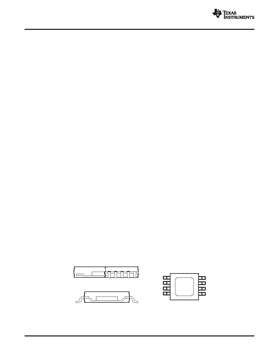
DIE
Side View (a)
End View (b)
Bottom View (c)
DIE
Thermal
Pad
SLOS224G – JULY 1999 – REVISED MARCH 2010
www.ti.com
CIRCUIT-LAYOUT CONSIDERATIONS
In order to achieve the levels of high-frequency performance of the THS403x, it is essential that proper
printed-circuit board (PCB) high-frequency design techniques be followed. A general set of guidelines is given
below. In addition, a THS403x evaluation board is available to use as a guide for layout or for evaluating the
device performance.
Ground planes: It is highly recommended that a ground plane be used on the board to provide all
components with a low inductive ground connection. However, in the areas of the amplifier inputs and output,
the ground plane can be removed to minimize the stray capacitance.
Proper power-supply decoupling: Use a 6.8-mF tantalum capacitor in parallel with a 0.1-mF ceramic capacitor
on each supply terminal. It may be possible to share the tantalum among several amplifiers depending on the
application, but a 0.1-mF ceramic capacitor should always be used on the supply terminal of every amplifier.
In addition, the 0.1-mF capacitor should be placed as close as possible to the supply terminal. As this distance
increases, the inductance in the connecting trace makes the capacitor less effective. The designer should
strive for distances of less than 0.1 inch between the device power terminals and the ceramic capacitors.
Sockets: Sockets are not recommended for high-speed operational amplifiers. The additional lead inductance
in the socket pins will often lead to stability problems. Surface-mount packages soldered directly to the
printed-circuit board is the best implementation.
Short trace runs/compact part placements: Optimum high-frequency performance is achieved when stray
series inductance has been minimized. To realize this, the circuit layout should be made as compact as
possible, thereby minimizing the length of all trace runs. Particular attention should be paid to the inverting
input of the amplifier. Its length should be kept as short as possible. This will help to minimize stray
capacitance at the input of the amplifier.
Surface-mount passive components: Using surface-mount passive components is recommended for
high-frequency amplifier circuits for several reasons. First, because of the extremely low lead inductance of
surface-mount components, the problem with stray series inductance is greatly reduced. Second, the small
size of surface-mount components naturally leads to a more compact layout thereby minimizing both stray
inductance and capacitance. If leaded components are used, it is recommended that the lead lengths be kept
as short as possible.
GENERAL PowerPAD DESIGN CONSIDERATIONS
The THS403x is available in a thermally-enhanced DGN package, which is a member of the PowerPAD family of
packages. This package is constructed using a downset leadframe upon which the die is mounted [see
Figure 60(a) and Figure 60(b)]. This arrangement results in the leadframe being exposed as a thermal pad on
the underside of the package [see Figure 60(c)]. Because this thermal pad has direct thermal contact with the
die, excellent thermal performance can be achieved by providing a good thermal path away from the thermal
pad.
The PowerPAD package allows for both assembly and thermal management in one manufacturing operation.
During the surface-mount solder operation (when the leads are being soldered), the thermal pad can also be
soldered to a copper area underneath the package. Through the use of thermal paths within this copper area,
heat can be conducted away from the package into either a ground plane or other heat-dissipating device.
The PowerPAD package represents a breakthrough in combining the small area and ease of assembly of
surface mount with the heretofore awkward mechanical methods of heatsinking.
A.
The thermal pad is electrically isolated from all terminals in the package.
Figure 60. Views of Thermally-Enhanced DGN Package
28
Copyright 1999–2010, Texas Instruments Incorporated
相关PDF资料 |
PDF描述 |
|---|---|
| 2065657-1 | CONN RCPT 80POS 8ROW RT ANG HM-Z |
| LT300303CR | FUSEBLOCK CLASS T 30A 3 POLE |
| LT300604CR | FUSEBLOCK CLASS T 60A 4 POLE |
| 213738-2 | CONN HEADER 19POS DRAWER GOLD |
| MAX4022EEE+T | IC BUFFER R-R 16-QSOP |
相关代理商/技术参数 |
参数描述 |
|---|---|
| THS4031IDGNR | 功能描述:高速运算放大器 100-MHz Low Noise Volt-Feedback Amp RoHS:否 制造商:Texas Instruments 通道数量:1 电压增益 dB:116 dB 输入补偿电压:0.5 mV 转换速度:55 V/us 工作电源电压:36 V 电源电流:7.5 mA 最大工作温度:+ 85 C 安装风格:SMD/SMT 封装 / 箱体:SOIC-8 封装:Tube |
| THS4031IDGNRG4 | 功能描述:高速运算放大器 100-MHz Low Noise Volt-Feedback Amp RoHS:否 制造商:Texas Instruments 通道数量:1 电压增益 dB:116 dB 输入补偿电压:0.5 mV 转换速度:55 V/us 工作电源电压:36 V 电源电流:7.5 mA 最大工作温度:+ 85 C 安装风格:SMD/SMT 封装 / 箱体:SOIC-8 封装:Tube |
| THS4031IDR | 功能描述:高速运算放大器 100-MHz Low Noise Volt-Feedback Amp RoHS:否 制造商:Texas Instruments 通道数量:1 电压增益 dB:116 dB 输入补偿电压:0.5 mV 转换速度:55 V/us 工作电源电压:36 V 电源电流:7.5 mA 最大工作温度:+ 85 C 安装风格:SMD/SMT 封装 / 箱体:SOIC-8 封装:Tube |
| THS4031IDRG4 | 功能描述:高速运算放大器 100-MHz Low Noise Volt-Feedback Amp RoHS:否 制造商:Texas Instruments 通道数量:1 电压增益 dB:116 dB 输入补偿电压:0.5 mV 转换速度:55 V/us 工作电源电压:36 V 电源电流:7.5 mA 最大工作温度:+ 85 C 安装风格:SMD/SMT 封装 / 箱体:SOIC-8 封装:Tube |
| THS4031JG | 制造商:TI 制造商全称:Texas Instruments 功能描述:100-MHz LOW-NOISE HIGH-SPEED AMPLIFIERS |
发布紧急采购,3分钟左右您将得到回复。