参数资料
| 型号: | THS4031IDGNG4 |
| 厂商: | Texas Instruments |
| 文件页数: | 22/47页 |
| 文件大小: | 0K |
| 描述: | IC OPAMP VFB 100MHZ SGL 8MSOP |
| 标准包装: | 80 |
| 放大器类型: | 电压反馈 |
| 电路数: | 1 |
| 转换速率: | 100 V/µs |
| -3db带宽: | 100MHz |
| 电流 - 输入偏压: | 3µA |
| 电压 - 输入偏移: | 500µV |
| 电流 - 电源: | 8.5mA |
| 电流 - 输出 / 通道: | 90mA |
| 电压 - 电源,单路/双路(±): | 9 V ~ 32 V,±4.5 V ~ 16 V |
| 工作温度: | -40°C ~ 85°C |
| 安装类型: | 表面贴装 |
| 封装/外壳: | 8-TSSOP,8-MSOP(0.118",3.00mm 宽)裸露焊盘 |
| 供应商设备封装: | 8-MSOP-PowerPad |
| 包装: | 管件 |
| 配用: | 296-10029-ND - EVAL MOD FOR THS4031 |
第1页第2页第3页第4页第5页第6页第7页第8页第9页第10页第11页第12页第13页第14页第15页第16页第17页第18页第19页第20页第21页当前第22页第23页第24页第25页第26页第27页第28页第29页第30页第31页第32页第33页第34页第35页第36页第37页第38页第39页第40页第41页第42页第43页第44页第45页第46页第47页
Thermal pad area (68 mils x 70 mils) with 5 vias
(Via diameter = 13 mils)
www.ti.com
SLOS224G – JULY 1999 – REVISED MARCH 2010
Although there are many ways to properly heatsink this device, the following steps illustrate the recommended
approach.
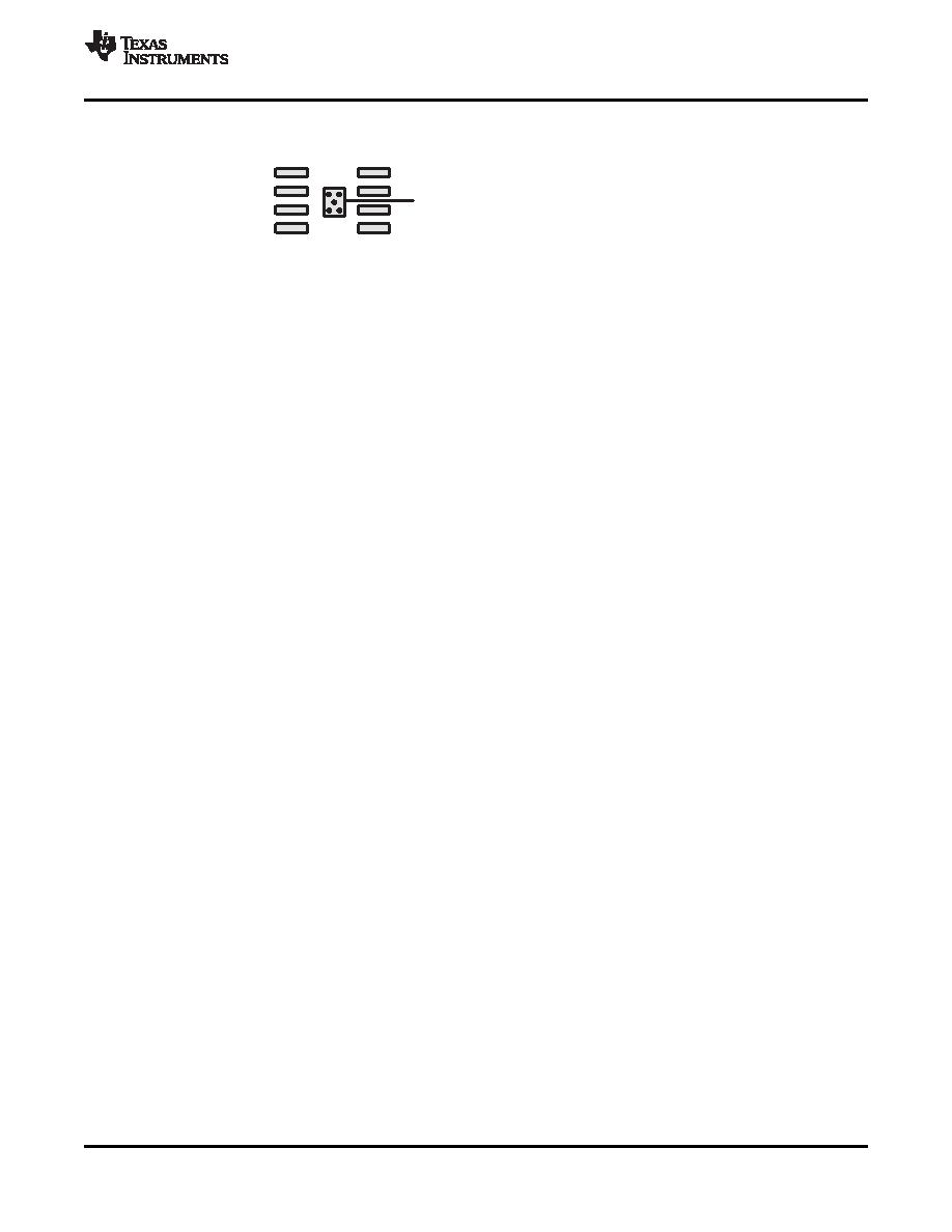
Figure 61. PowerPAD PCB Etch and Via Pattern
1. Prepare the PCB with a top-side etch pattern as shown in Figure 61. There should be etch for the leads as
well as etch for the thermal pad.
2. Place five holes in the area of the thermal pad. These holes should be 13 mils (0,3302 mm) in diameter.
They are kept small so that solder wicking through the holes is not a problem during reflow.
3. Additional vias may be placed anywhere along the thermal plane outside of the thermal pad area. This helps
dissipate the heat generated by the THS403xDGN IC. These additional vias may be larger than the 13-mil
diameter vias directly under the thermal pad. They can be larger because they are not in the thermal pad
area to be soldered so that wicking is not a problem.
4. Connect all holes to the internal ground plane.
5. When connecting these holes to the ground plane, do not use the typical web or spoke via connection
methodology. Web connections have a high thermal-resistance connection that is useful for slowing the heat
transfer during soldering operations. This makes the soldering of vias that have plane connections easier. In
this application, however, low thermal resistance is desired for the most efficient heat transfer. Therefore, the
holes under the THS403xDGN package should connect to the internal ground plane with a complete
connection around the entire circumference of the plated-through hole.
6. The top-side solder mask should leave the terminals of the package and the thermal pad area with its five
holes exposed. The bottom-side solder mask should cover the five holes of the thermal pad area, which
prevents solder from being pulled away from the thermal pad area during the reflow process.
7. Apply solder paste to the exposed thermal pad area and to all the IC terminals.
8. With these preparatory steps in place, the THS403xDGN IC is simply placed in position and run through the
solder reflow operation as any standard surface-mount component. This results in a part that is properly
installed.
Copyright 1999–2010, Texas Instruments Incorporated
29
相关PDF资料 |
PDF描述 |
|---|---|
| 2065657-1 | CONN RCPT 80POS 8ROW RT ANG HM-Z |
| LT300303CR | FUSEBLOCK CLASS T 30A 3 POLE |
| LT300604CR | FUSEBLOCK CLASS T 60A 4 POLE |
| 213738-2 | CONN HEADER 19POS DRAWER GOLD |
| MAX4022EEE+T | IC BUFFER R-R 16-QSOP |
相关代理商/技术参数 |
参数描述 |
|---|---|
| THS4031IDGNR | 功能描述:高速运算放大器 100-MHz Low Noise Volt-Feedback Amp RoHS:否 制造商:Texas Instruments 通道数量:1 电压增益 dB:116 dB 输入补偿电压:0.5 mV 转换速度:55 V/us 工作电源电压:36 V 电源电流:7.5 mA 最大工作温度:+ 85 C 安装风格:SMD/SMT 封装 / 箱体:SOIC-8 封装:Tube |
| THS4031IDGNRG4 | 功能描述:高速运算放大器 100-MHz Low Noise Volt-Feedback Amp RoHS:否 制造商:Texas Instruments 通道数量:1 电压增益 dB:116 dB 输入补偿电压:0.5 mV 转换速度:55 V/us 工作电源电压:36 V 电源电流:7.5 mA 最大工作温度:+ 85 C 安装风格:SMD/SMT 封装 / 箱体:SOIC-8 封装:Tube |
| THS4031IDR | 功能描述:高速运算放大器 100-MHz Low Noise Volt-Feedback Amp RoHS:否 制造商:Texas Instruments 通道数量:1 电压增益 dB:116 dB 输入补偿电压:0.5 mV 转换速度:55 V/us 工作电源电压:36 V 电源电流:7.5 mA 最大工作温度:+ 85 C 安装风格:SMD/SMT 封装 / 箱体:SOIC-8 封装:Tube |
| THS4031IDRG4 | 功能描述:高速运算放大器 100-MHz Low Noise Volt-Feedback Amp RoHS:否 制造商:Texas Instruments 通道数量:1 电压增益 dB:116 dB 输入补偿电压:0.5 mV 转换速度:55 V/us 工作电源电压:36 V 电源电流:7.5 mA 最大工作温度:+ 85 C 安装风格:SMD/SMT 封装 / 箱体:SOIC-8 封装:Tube |
| THS4031JG | 制造商:TI 制造商全称:Texas Instruments 功能描述:100-MHz LOW-NOISE HIGH-SPEED AMPLIFIERS |
发布紧急采购,3分钟左右您将得到回复。