- 您现在的位置:买卖IC网 > PDF目录98224 > THS4081IDGNR (TEXAS INSTRUMENTS INC) 1 CHANNEL, VIDEO AMPLIFIER, PDSO8 PDF资料下载
参数资料
| 型号: | THS4081IDGNR |
| 厂商: | TEXAS INSTRUMENTS INC |
| 元件分类: | 音频/视频放大 |
| 英文描述: | 1 CHANNEL, VIDEO AMPLIFIER, PDSO8 |
| 封装: | GREEN, PLASTIC, MSOP-8 |
| 文件页数: | 11/32页 |
| 文件大小: | 841K |
| 代理商: | THS4081IDGNR |
第1页第2页第3页第4页第5页第6页第7页第8页第9页第10页当前第11页第12页第13页第14页第15页第16页第17页第18页第19页第20页第21页第22页第23页第24页第25页第26页第27页第28页第29页第30页第31页第32页
THS4081, THS4082
175MHz LOW POWER HIGHSPEED AMPLIFIERS
SLOS274D DECEMBER 1999 REVISED JUNE 2001
19
POST OFFICE BOX 655303
DALLAS, TEXAS 75265
APPLICATION INFORMATION
general PowerPAD
design considerations (continued)
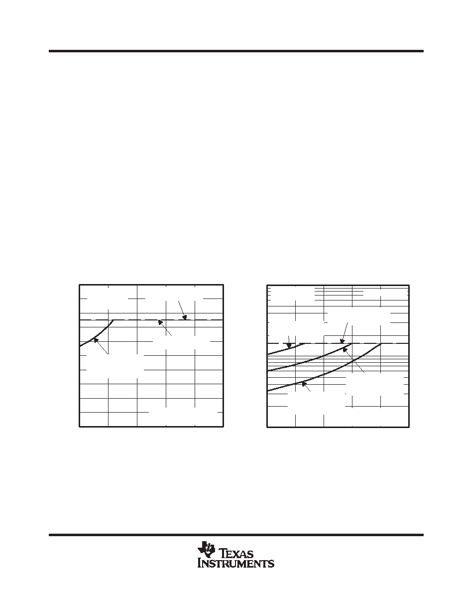
The next consideration is the package constraints. The two sources of heat within an amplifier are quiescent
power and output power. The designer should never forget about the quiescent heat generated within the
device, especially multiamplifier devices. Because these devices have linear output stages (Class A-B), most
of the heat dissipation is at low output voltages with high output currents. Figure 47 to Figure 50 show this effect,
along with the quiescent heat, with an ambient air temperature of 50
°C. Obviously, as the ambient temperature
increases, the limit lines shown will drop accordingly. The area under each respective limit line is considered
the safe operating area. Any condition above this line will exceed the amplifier’s limits and failure may result.
When using VCC = ±5 V, there is generally not a heat problem, even with SOIC packages. But, when using
VCC = ±15 V, the SOIC package is severely limited in the amount of heat it can dissipate. The other key factor
when looking at these graphs is how the devices are mounted on the PCB. The PowerPAD
devices are
extremely useful for heat dissipation. But, the device should always be soldered to a copper plane to fully use
the heat dissipation properties of the PowerPAD
. The SOIC package, on the other hand, is highly dependent
on how it is mounted on the PCB. As more trace and copper area is placed around the device,
θJA decreases
and the heat dissipation capability increases. The currents and voltages shown in these graphs are for the total
package. For the dual amplifier package (THS4082), the sum of the RMS output currents and voltages should
be used to choose the proper package. The graphs shown assume that both amplifier’s outputs are identical.
Figure 47
Package With
θJA < = 127°C/W
SO-8 Package
θJA = 167°C/W
Low-K Test PCB
VCC = ± 5 V
TJ = 150°C
TA = 50°C
100
80
40
0
01
2
3
Maximum
RMS
Output
Current
mA
140
180
200
45
160
120
60
20
| VO | RMS Output Voltage V
I O||
Maximum Output
Current Limit Line
THS4081
MAXIMUM RMS OUTPUT CURRENT
vs
RMS OUTPUT VOLTAGE DUE TO THERMAL LIMITS
Safe Operating
Area
Figure 48
100
10
03
6
9
1000
12
15
Maximum Output
Current Limit Line
SO-8 Package
θJA = 167°C/W
Low-K Test PCB
SO-8 Package
θJA = 98°C/W
High-K Test PCB
TJ = 150°C
TA = 50°C
| VO | RMS Output Voltage V
Maximum
RMS
Output
Current
mA
I O||
VCC = ± 15 V
DGN Package
θJA = 58.4°C/W
THS4081
MAXIMUM RMS OUTPUT CURRENT
vs
RMS OUTPUT VOLTAGE DUE TO THERMAL LIMITS
Safe Operating
Area
相关PDF资料 |
PDF描述 |
|---|---|
| THS4081IDGN | 1 CHANNEL, VIDEO AMPLIFIER, PDSO8 |
| THS4081IDR | 1 CHANNEL, VIDEO AMPLIFIER, PDSO8 |
| THS4081ID | 1 CHANNEL, VIDEO AMPLIFIER, PDSO8 |
| THS4081CDG4 | 1 CHANNEL, VIDEO AMPLIFIER, PDSO8 |
| THS4081CDGNG4 | 1 CHANNEL, VIDEO AMPLIFIER, PDSO8 |
相关代理商/技术参数 |
参数描述 |
|---|---|
| THS4081IDGNRG4 | 功能描述:高速运算放大器 175-MHz Low-Power Volt-Feedback Amp RoHS:否 制造商:Texas Instruments 通道数量:1 电压增益 dB:116 dB 输入补偿电压:0.5 mV 转换速度:55 V/us 工作电源电压:36 V 电源电流:7.5 mA 最大工作温度:+ 85 C 安装风格:SMD/SMT 封装 / 箱体:SOIC-8 封装:Tube |
| THS4082 | 制造商:TI 制造商全称:Texas Instruments 功能描述:175-MHz LOW-POWER HIGH-SPEED AMPLIFIERS |
| THS4082CD | 功能描述:高速运算放大器 Dual 175MHz RoHS:否 制造商:Texas Instruments 通道数量:1 电压增益 dB:116 dB 输入补偿电压:0.5 mV 转换速度:55 V/us 工作电源电压:36 V 电源电流:7.5 mA 最大工作温度:+ 85 C 安装风格:SMD/SMT 封装 / 箱体:SOIC-8 封装:Tube |
| THS4082CDG4 | 功能描述:高速运算放大器 175-MHz Low-Power Vltg-Feedback Dual RoHS:否 制造商:Texas Instruments 通道数量:1 电压增益 dB:116 dB 输入补偿电压:0.5 mV 转换速度:55 V/us 工作电源电压:36 V 电源电流:7.5 mA 最大工作温度:+ 85 C 安装风格:SMD/SMT 封装 / 箱体:SOIC-8 封装:Tube |
| THS4082CDGN | 制造商:Rochester Electronics LLC 功能描述:LOW POWER, VF, DUAL OP-AMP - Bulk |
发布紧急采购,3分钟左右您将得到回复。