- 您现在的位置:买卖IC网 > PDF目录384977 > TIP36B (ON SEMICONDUCTOR) Complementary Silicon High(互补型硅高功率晶体管) PDF资料下载
参数资料
| 型号: | TIP36B |
| 厂商: | ON SEMICONDUCTOR |
| 元件分类: | 功率晶体管 |
| 英文描述: | Complementary Silicon High(互补型硅高功率晶体管) |
| 中文描述: | 25 A, 80 V, PNP, Si, POWER TRANSISTOR, TO-218 |
| 封装: | CASE 340D-02, 3 PIN |
| 文件页数: | 4/6页 |
| 文件大小: | 80K |
| 代理商: | TIP36B |
TIP35A, TIP35B, TIP35C (NPN); TIP36A, TIP36B, TIP36C (PNP)
http://onsemi.com
4
0.5
1.0
2.0
7.0
0.3
3.0
5.0
0.7
I
C
, COLLECTOR CURRENT (AMPERES)
Figure 4. TurnOff Time
10
7.0
5.0
t
3.0
2.0
1.0
0.7
0.5
0.3
0.2
0.1
10
20
30
T
J
= 25
°
C
V
CC
= 30 V
I
C
/I
B
= 10
I
B1
= I
B2
t
s
t
f
(PNP)
(NPN)
t
s
t
f
I
C
, COLLECTOR CURRENT (AMPS)
h
Figure 5. DC Current Gain
200
500
0.2
0.5
2.0
100
0.1
100
50
20
10
1.0
V
CE
= 4.0 V
T
J
= 25
°
C
5.0
10
20
5.0
50
PNP
NPN
1000
2.0
1.0
FORWARD BIAS
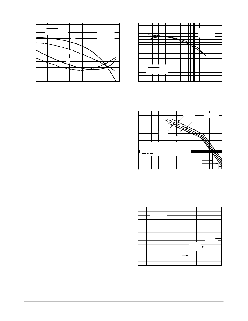
There are two limitations on the power handling ability of
a transistor: average junction temperature and second
breakdown. Safe operating area curves indicate I
C
V
CE
limits of the transistor that must be observed for reliable
operation; i.e., the transistor must not be subjected to greater
dissipation than the curves indicate.
The data of Figure 6 is based on T
C
= 25 C; T
J(pk)
is
variable depending on power level. Second breakdown
pulse limits are valid for duty cycles to 10% but must be
derated when T
C
25 C. Second breakdown limitations do
not derate the same as thermal limitations.
REVERSE BIAS
For inductive loads, high voltage and high current must be
sustained simultaneously during turnoff, in most cases,
with the base to emitter junction reverse biased. Under these
conditions the collector voltage must be held to a safe level
at or below a specific value of collector current. This can be
accomplished by several means such as active clamping, RC
snubbing, load line shaping, etc. The safe level for these
devices is specified as Reverse Bias Safe Operating Area
and represents the voltagecurrent conditions during
reverse biased turnoff. This rating is verified under
clamped conditions so that the device is never subjected to
an avalanche mode. Figure 7 gives RBSOA characteristics.
V
CE
, COLLECTOREMITTER VOLTAGE (VOLTS)
7.0
20
1.0
50
100
0.2
0
0.5
0.3
SECONDARY BREAKDOWN
THERMAL LIMIT
BONDING WIRE LIMIT
1.0ms
dc
300 s
2.0
1.0
100
30
20
I
10ms
Figure 6. Maximum Rated Forward Bias
Safe Operating Area
50
10
5.0
2.0
3.0
5.0
10
30
70
T
C
= 25
°
C
TIP35A, 36A
TIP35B, 36B
TIP35C, 36C
V
CE
, COLLECTOREMITTER VOLTAGE (VOLTS)
40
60
0
80
100
5.0
0
15
20
40
30
I
Figure 7. Maximum Rated Forward Bias
Safe Operating Area
25
10
10
20
30
50
70
90
T
J
≤
100
°
C
TIP35A
TIP36A
TIP35B
TIP36B
TIP35C
TIP36C
相关PDF资料 |
PDF描述 |
|---|---|
| TIP36C | Complementary Silicon High(互补型硅高功率晶体管) |
| TIP35A | Complementary Silicon High(互补型硅高功率晶体管) |
| TIP35B | Complementary Silicon High(互补型硅高功率晶体管) |
| TIP35C | Complementary Silicon High(互补型硅高功率晶体管) |
| TIP36A | Complementary Silicon High(互补型硅高功率晶体管) |
相关代理商/技术参数 |
参数描述 |
|---|---|
| TIP36BG | 制造商:ONSEMI 制造商全称:ON Semiconductor 功能描述:Complementary Silicon High?Power Transistors |
| TIP36B-S | 功能描述:两极晶体管 - BJT 80V 25A PNP RoHS:否 制造商:STMicroelectronics 配置: 晶体管极性:PNP 集电极—基极电压 VCBO: 集电极—发射极最大电压 VCEO:- 40 V 发射极 - 基极电压 VEBO:- 6 V 集电极—射极饱和电压: 最大直流电集电极电流: 增益带宽产品fT: 直流集电极/Base Gain hfe Min:100 A 最大工作温度: 安装风格:SMD/SMT 封装 / 箱体:PowerFLAT 2 x 2 |
| TIP36C | 功能描述:两极晶体管 - BJT PNP Gen Pur Power RoHS:否 制造商:STMicroelectronics 配置: 晶体管极性:PNP 集电极—基极电压 VCBO: 集电极—发射极最大电压 VCEO:- 40 V 发射极 - 基极电压 VEBO:- 6 V 集电极—射极饱和电压: 最大直流电集电极电流: 增益带宽产品fT: 直流集电极/Base Gain hfe Min:100 A 最大工作温度: 安装风格:SMD/SMT 封装 / 箱体:PowerFLAT 2 x 2 |
| TIP36C | 制造商:Bourns Inc 功能描述:TRANSISTOR PNP SOT-93 制造商:SPC Multicomp 功能描述:TRANSISTOR PNP SOT-93 |
| TIP36C_01 | 制造商:KEC 制造商全称:KEC(Korea Electronics) 功能描述:TRIPLE DIFFUSED PNP TRANSISTOR |
发布紧急采购,3分钟左右您将得到回复。