- 您现在的位置:买卖IC网 > PDF目录299979 > TK7403232LCLEX (TOKO INC) DUAL OUTPUT, FIXED POSITIVE LDO REGULATOR, PDSO8 PDF资料下载
参数资料
| 型号: | TK7403232LCLEX |
| 厂商: | TOKO INC |
| 元件分类: | 固定正电压多路输出LDO稳压器 |
| 英文描述: | DUAL OUTPUT, FIXED POSITIVE LDO REGULATOR, PDSO8 |
| 封装: | SOT-23, 8 PIN |
| 文件页数: | 4/30页 |
| 文件大小: | 913K |
| 代理商: | TK7403232LCLEX |
第1页第2页第3页当前第4页第5页第6页第7页第8页第9页第10页第11页第12页第13页第14页第15页第16页第17页第18页第19页第20页第21页第22页第23页第24页第25页第26页第27页第28页第29页第30页
TOKO@Inc.
IC Data Sheet
TK740xxL
May 2001
GC3-H010 /D
Page 12
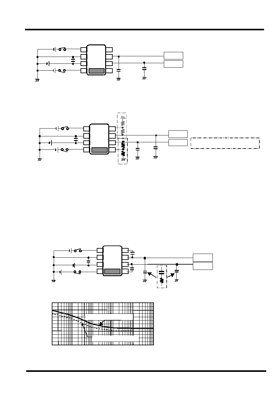
Standard Application
Typically, give the capacitor as
large a value as practical in
consideration of the temperature
characteristic. The output noise
and ripple noise decrease with a
larger
capacitance
value.
In
addition, the response to the output
side load change also improves.
Output voltage change
The output voltage on both sides can be set by using R1 and R2. The output voltage is decided by the ratio
of R1 and R2. The error of the output voltage usually grows.
Noise reduction (Improvement of ripple rejection ratio)
Please connect Cfb with the FbA terminals (1 and 2) and the FbB terminals (3 and 4). It is possible to use Cfb
only on the needed side.
The tantalum capacitor is the best in this application. A small
capacitance is sufficient (0.1
F, 0.22F, etc.). When the ceramic capacitor is used, the noise grows in the low
current region. If 1.0.( Rs1) is connected in series with the ceramic capacitor, the same characteristics as
a tantalum capacitor can be obtained. Please adjust the output side capacitor to the value in which stable
operation is done over all required temperature ranges. Damage will not be caused by enlarging this value.
Increasing this value will decrease the ripple noise and improve the output load transient response. However,
the risetime using the on/off control becomes slower. It is possible to use the noise reduction application with
the output voltage change application above.
ContB
u in
CL A 1.0 ε
1
4
5
8
CL B 1.0 F
GND
VoutB
VoutA
ContA
0.1
F
Cfb
Cfb =4700pF
We recommend 4700pF for Cfb
0
100
10000
200
1000
100
Noise
(V)
@Iout=50`200mA
Cfb(pF)
TK74028
Cfb@VS@Noise Level (A=B)
100000
CL=1.0
F@Tantalum
CL=1.0
F@MLCC
10
1
ContB
Vout
iR1 R2 +1 j~ 1.19
22k R2
R1(K ) (Vout 1.19 |1) ~
R2
u
in
CL B
0.1 F
(1.0 F)
GND
1
4
5
8
CL A
0.22 F
(1.0 F)
VoutB
VoutA
ContA
0.1
F
R1
R2
R2f
R1f
u in
CL A
0.1 ε
(1.0 F)
GND
1
4
5
8
CL B
0.1 F
(1.0 F)
VoutB
VoutA
ContA
ContB
0.1
F
相关PDF资料 |
PDF描述 |
|---|---|
| TK7403535LCLEX | DUAL OUTPUT, FIXED POSITIVE LDO REGULATOR, PDSO8 |
| TK740SIL-2626 | DUAL OUTPUT, FIXED POSITIVE LDO REGULATOR, PDSO8 |
| TK740SIL-2727 | DUAL OUTPUT, FIXED POSITIVE LDO REGULATOR, PDSO8 |
| TL12W03-L(T30) | SINGLE COLOR LED, WARM WHITE |
| TL6700AF160QJ | KEYPAD SWITCH, SPST, MOMENTARY, 0.05A, 12VDC, 2.06 N, SURFACE MOUNT-STRAIGHT |
相关代理商/技术参数 |
参数描述 |
|---|---|
| TK7408 | 制造商:Tekmos 功能描述:IC, PLCC-44 |
| TK75 | 制造商:ALTECH 制造商全称:Altech corporation 功能描述:POLYCARBONATE ENCLOSURE TK 75 |
| TK7500 | 功能描述:冲压机与冲模 FRM W/4 DIES & CASE RoHS:否 制造商:Souriau 大小: 产品:Dies 类型:Crimping 描述/功能: |
| TK75001 | 制造商:TOKO 制造商全称:TOKO, Inc 功能描述:PWM CONTROLLER |
| TK75001D | 制造商:TOKO 制造商全称:TOKO, Inc 功能描述:PWM CONTROLLER |
发布紧急采购,3分钟左右您将得到回复。