- 您现在的位置:买卖IC网 > PDF目录97203 > TLC1551INW (TEXAS INSTRUMENTS INC) 1-CH 10-BIT SUCCESSIVE APPROXIMATION ADC, PARALLEL ACCESS, PDIP24 PDF资料下载
参数资料
| 型号: | TLC1551INW |
| 厂商: | TEXAS INSTRUMENTS INC |
| 元件分类: | ADC |
| 英文描述: | 1-CH 10-BIT SUCCESSIVE APPROXIMATION ADC, PARALLEL ACCESS, PDIP24 |
| 封装: | PLASTIC, DIP-24 |
| 文件页数: | 4/10页 |
| 文件大小: | 141K |
| 代理商: | TLC1551INW |
TLC1550I, TLC1550M, TLC1551I
10-BIT ANALOG-TO-DIGITAL CONVERTERS
WITH PARALLEL OUTPUTS
SLAS043F – MAY 1991 – REVISED JANUARY 2003
3
POST OFFICE BOX 655303
DALLAS, TEXAS 75265
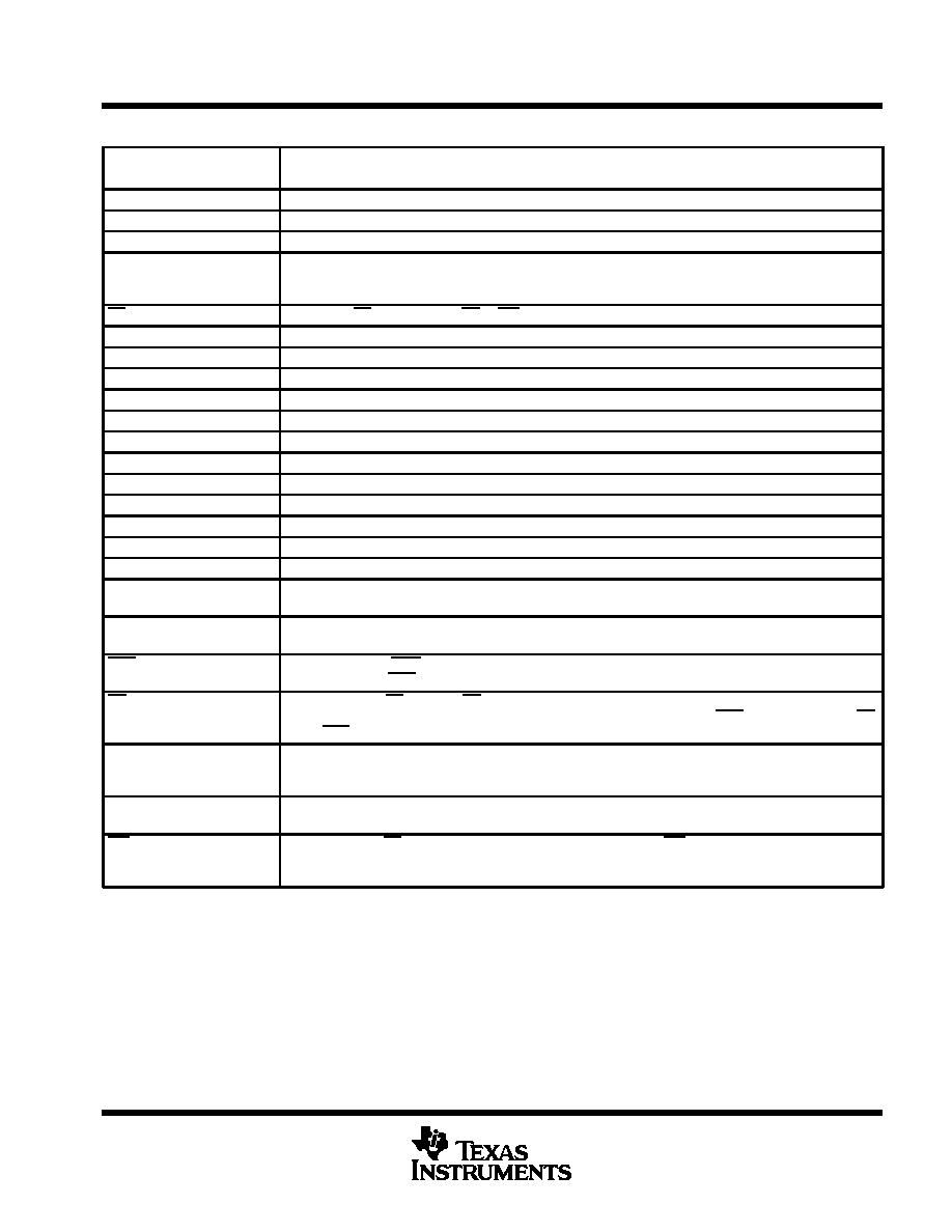
Terminal Functions
TERMINAL
DESCRIPTION
NAME
NO.
DESCRIPTION
ANLG GND
4
3
Analog ground. The reference point for the voltage applied on terminals ANLG VDD, AIN, REF+, and REF–.
AIN
5
4
Analog voltage input. The voltage applied to AIN is converted to the equivalent digital output.
ANLG VDD
6
5
Analog positive power supply voltage. The voltage applied to this terminal is designated VDD3.
CLKIN
26
22
Clock input. CLKIN is used for external clocking instead of using the internal system clock. It usually takes a
few microseconds before the internal clock is disabled. To use the internal clock, CLKIN should be tied high
or left unconnected.
CS
25
21
Chip-select. CS must be low for RD or WR to be recognized by the A/D converter.
D0
13
11
Data bus output. D0 is bit 1 (LSB).
D1
14
12
Data bus output. D1 is bit 2.
D2
16
13
Data bus output. D2 is bit 3.
D3
17
14
Data bus output. D3 is bit 4.
D4
18
15
Data bus output. D4 is bit 5.
D5
19
16
Data bus output. D5 is bit 6.
D6
20
17
Data bus output. D6 is bit 7.
D7
21
18
Data bus output. D7 is bit 8.
D8
23
19
Data bus output. D8 is bit 9.
D9
24
20
Data bus output. D9 is bit 10 (MSB).
DGTL GND1
7
6
Digital ground 1. The ground for power supply DGTL VDD1 and is the substrate connection
DGTL GND2
9
7
Digital ground 2. The ground for power supply DGTL VDD2
DGTL VDD1
10
8
Digital positive power-supply voltage 1. DGTL VDD1 supplies the logic. The voltage applied to DGTL VDD1 is
designated VDD1.
DGTL VDD2
11
9
Digital positive power-supply voltage 2. DGTL VDD2 supplies only the higher-current output buffers. The voltage
applied to DGTL VDD2 is designated VDD2.
EOC
12
10
End-of-conversion. EOC goes low indicating that conversion is complete and the results have been transferred
to the output latch. EOC can be connected to the
P- or DSP-interrupt terminal or can be continuously polled.
RD
28
24
Read input. When CS is low and RD is taken low, the data is placed on the data bus from the output latch. The
output latch stores the conversion results at the most recent negative edge of EOC. The falling edge of RD
resets EOC to a high within the td(EOC) specifications.
REF+
2
1
Positive voltage-reference input. Any analog input that is greater than or equal to the voltage on REF+ converts
to 1111111111. Analog input voltages between REF + and REF – convert to the appropriate result in a ratiometric
manner.
REF –
3
2
Negative voltage reference input. Any analog input that is less than or equal to the voltage on REF – converts
to 0000000000.
WR
27
23
Write input. When CS is low, conversion is started on the rising edge of WR. On this rising edge, the ADC holds
the analog input until conversion is completed. Before and after the conversion period, which is given by t conv,
the ADC remains in the sampling mode.
Terminal numbers for FK and FN packages.
Terminal numbers for J, DW, and NW packages.
相关PDF资料 |
PDF描述 |
|---|---|
| TLC2934IPW | PHASE LOCKED LOOP, 130 MHz, PDSO14 |
| TLC4016MN | QUAD 1-CHANNEL, SGL POLE SGL THROW SWITCH, PDIP14 |
| TLC532AIFN | 8-BIT SUCCESSIVE APPROXIMATION ADC, PARALLEL ACCESS, PQCC28 |
| TLC532AIN | 8-BIT SUCCESSIVE APPROXIMATION ADC, PARALLEL ACCESS, PDIP28 |
| TLC533AIFN | 8-BIT SUCCESSIVE APPROXIMATION ADC, PARALLEL ACCESS, PQCC28 |
相关代理商/技术参数 |
参数描述 |
|---|---|
| TLC1553-1 | 制造商:Pulse 功能描述:TRANSFORMERS - Rail/Tube |
| TLC1553-2 | 制造商:Pulse 功能描述:TRANSFORMERS - Rail/Tube |
| TLC1553-3 | 制造商:Pulse 功能描述:TRANSFORMERS - Rail/Tube |
| TLC1553-40 | 制造商:Pulse Electronics Corporation 功能描述:TRANSFORMERS - Rail/Tube |
| TLC1553-45 | 制造商:Pulse 功能描述:PULSE TX 1CT:2.5CT/1CT:1.79CT 100VRMS 1OHM PRIM. DCR 3.5OHM - Rail/Tube |
发布紧急采购,3分钟左右您将得到回复。