- 您现在的位置:买卖IC网 > PDF目录98236 > TLC2543QDWRQ1 (TEXAS INSTRUMENTS INC) 11-CH 12-BIT SUCCESSIVE APPROXIMATION ADC, SERIAL ACCESS, PDSO20 PDF资料下载
参数资料
| 型号: | TLC2543QDWRQ1 |
| 厂商: | TEXAS INSTRUMENTS INC |
| 元件分类: | ADC |
| 英文描述: | 11-CH 12-BIT SUCCESSIVE APPROXIMATION ADC, SERIAL ACCESS, PDSO20 |
| 封装: | PLASTIC, SOIC-20 |
| 文件页数: | 10/25页 |
| 文件大小: | 413K |
| 代理商: | TLC2543QDWRQ1 |
TLC2543Q1
12BIT ANALOGTODIGITAL CONVERTERS
WITH SERIAL CONTROL AND 11 ANALOG INPUTS
SGLS218D NOVEMBER 2003 REVISED MAY 2008
18
POST OFFICE BOX 655303
DALLAS, TEXAS 75265
PRINCIPLES OF OPERATION
analog input, test, and power-down mode
The 11 analog inputs, three internal voltages, and power-down mode are selected by the input multiplexer
according to the input addresses shown in Table 3, Table 4, and Table 5. The input multiplexer is a
break-before-make type to reduce input-to-input noise rejection resulting from channel switching. Sampling of
the analog input starts on the falling edge of the fourth I/O CLOCK and continues for the remaining I/O CLOCK
pulses. The sample is held on the falling edge of the last I/O CLOCK pulse. The three internal test inputs are
applied to the multiplexer, then sampled and converted in the same manner as the external analog inputs. The
first conversion after the device has returned from the power-down state may not read accurately due to internal
device settling.
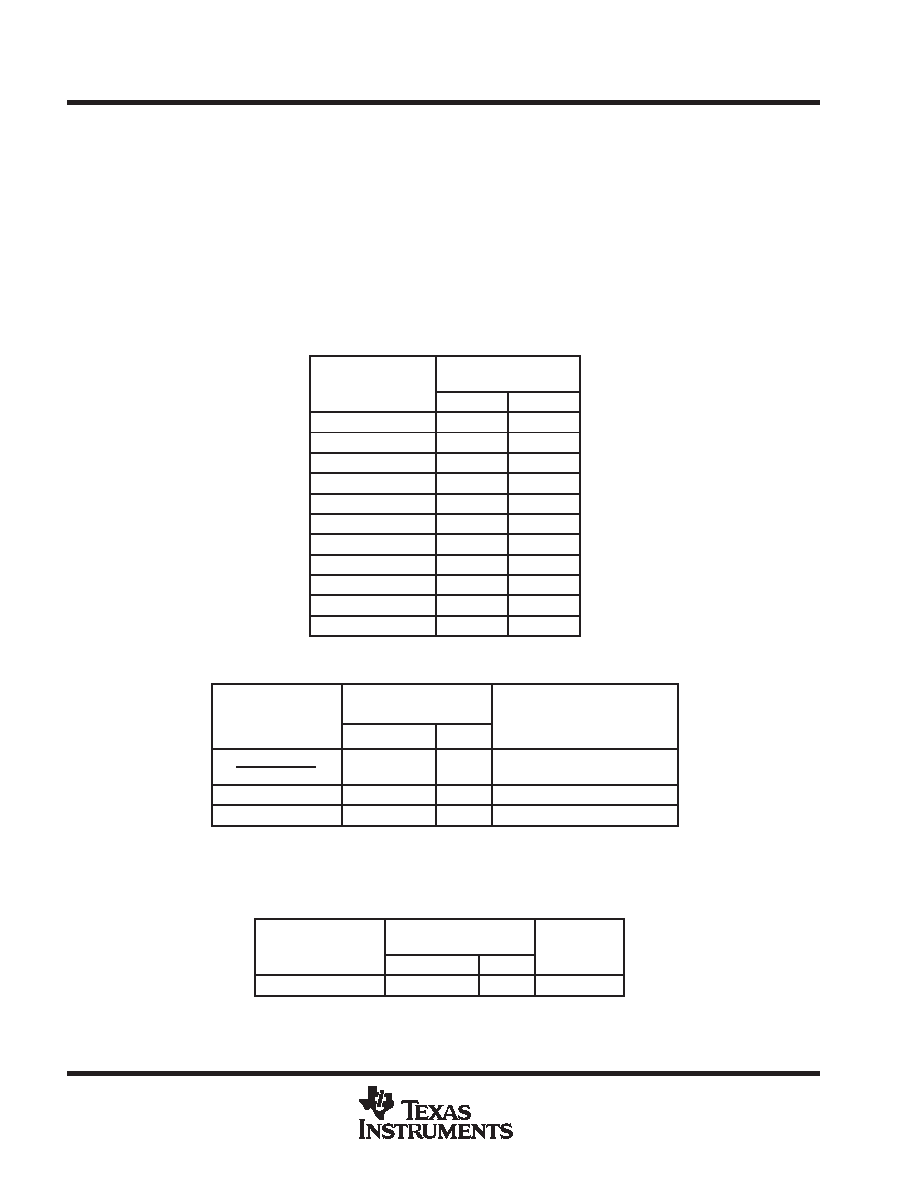
Table 3. Analog-Channel-Select Address
ANALOG INPUT
SELECTED
VALUE SHIFTED INTO
DATA INPUT
SELECTED
BINARY
HEX
AIN0
0000
0
AIN1
0001
1
AIN2
0010
2
AIN3
0011
3
AIN4
0100
4
AIN5
0101
5
AIN6
0110
6
AIN7
0111
7
AIN8
1000
8
AIN9
1001
9
AIN10
1010
A
Table 4. Test-Mode-Select Address
INTERNAL
SELF-TEST
VOLTAGE
VALUE SHIFTED INTO
DATA INPUT
UNIPOLAR OUTPUT
RESULT (HEX)
VOLTAGE
SELECTED
BINARY
HEX
RESULT (HEX)
Vref + Vref
2
1011
B
800
Vref
1100
C
000
Vref +
1101
D
FFF
Vref+ is the voltage applied to REF+, and Vref is the voltage applied to REF.
The output results shown are the ideal values and may vary with the reference stability
and with internal offsets.
Table 5. Power-Down-Select Address
INPUT COMMAND
VALUE SHIFTED INTO
DATA INPUT
RESULT
INPUT COMMAND
BINARY
HEX
RESULT
Power down
1110
E
ICC ≤ 25 A
相关PDF资料 |
PDF描述 |
|---|---|
| TLC2543MDBREP | 11-CH 12-BIT SUCCESSIVE APPROXIMATION ADC, SERIAL ACCESS, PDSO20 |
| TLC2543QDWREP | 11-CH 12-BIT SUCCESSIVE APPROXIMATION ADC, SERIAL ACCESS, PDSO20 |
| TLC2543MFK | 11-CH 12-BIT SUCCESSIVE APPROXIMATION ADC, SERIAL ACCESS, CQCC20 |
| TLC2552IDGK | 2-CH 12-BIT SUCCESSIVE APPROXIMATION ADC, SERIAL ACCESS, PDSO8 |
| TLC2552IDR | 2-CH 12-BIT SUCCESSIVE APPROXIMATION ADC, SERIAL ACCESS, PDSO8 |
相关代理商/技术参数 |
参数描述 |
|---|---|
| TLC254ACD | 功能描述:运算放大器 - 运放 Quad LinCMOS RoHS:否 制造商:STMicroelectronics 通道数量:4 共模抑制比(最小值):63 dB 输入补偿电压:1 mV 输入偏流(最大值):10 pA 工作电源电压:2.7 V to 5.5 V 安装风格:SMD/SMT 封装 / 箱体:QFN-16 转换速度:0.89 V/us 关闭:No 输出电流:55 mA 最大工作温度:+ 125 C 封装:Reel |
| TLC254ACDG4 | 功能描述:运算放大器 - 运放 LinCMOS Quad OP AMP RoHS:否 制造商:STMicroelectronics 通道数量:4 共模抑制比(最小值):63 dB 输入补偿电压:1 mV 输入偏流(最大值):10 pA 工作电源电压:2.7 V to 5.5 V 安装风格:SMD/SMT 封装 / 箱体:QFN-16 转换速度:0.89 V/us 关闭:No 输出电流:55 mA 最大工作温度:+ 125 C 封装:Reel |
| TLC254ACN | 功能描述:运算放大器 - 运放 Lin CMOS Quad RoHS:否 制造商:STMicroelectronics 通道数量:4 共模抑制比(最小值):63 dB 输入补偿电压:1 mV 输入偏流(最大值):10 pA 工作电源电压:2.7 V to 5.5 V 安装风格:SMD/SMT 封装 / 箱体:QFN-16 转换速度:0.89 V/us 关闭:No 输出电流:55 mA 最大工作温度:+ 125 C 封装:Reel |
| TLC254ACNE4 | 功能描述:运算放大器 - 运放 LinCMOS Quad Op Amp RoHS:否 制造商:STMicroelectronics 通道数量:4 共模抑制比(最小值):63 dB 输入补偿电压:1 mV 输入偏流(最大值):10 pA 工作电源电压:2.7 V to 5.5 V 安装风格:SMD/SMT 封装 / 箱体:QFN-16 转换速度:0.89 V/us 关闭:No 输出电流:55 mA 最大工作温度:+ 125 C 封装:Reel |
| TLC254BCD | 功能描述:运算放大器 - 运放 LinCMOS Quad RoHS:否 制造商:STMicroelectronics 通道数量:4 共模抑制比(最小值):63 dB 输入补偿电压:1 mV 输入偏流(最大值):10 pA 工作电源电压:2.7 V to 5.5 V 安装风格:SMD/SMT 封装 / 箱体:QFN-16 转换速度:0.89 V/us 关闭:No 输出电流:55 mA 最大工作温度:+ 125 C 封装:Reel |
发布紧急采购,3分钟左右您将得到回复。