- 您现在的位置:买卖IC网 > PDF目录382606 > TLC372Y (Texas Instruments, Inc.) LinCMOSE DUAL DIFFERENTIAL COMPARATORS PDF资料下载
参数资料
| 型号: | TLC372Y |
| 厂商: | Texas Instruments, Inc. |
| 元件分类: | 比较器 |
| 英文描述: | LinCMOSE DUAL DIFFERENTIAL COMPARATORS |
| 中文描述: | LinCMOSE双差分比较器 |
| 文件页数: | 6/12页 |
| 文件大小: | 183K |
| 代理商: | TLC372Y |
TLC372, TLC372Q, TLC372Y
LinCMOS
DUAL DIFFERENTIAL COMPARATORS
SLCS114B – NOVEMBER 1983 – REVISED MARCH 1999
6
POST OFFICE BOX 655303
DALLAS, TEXAS 75265
electrical characteristics at specified free-air temperature, V
DD
= 5 V, T
A
= 25
°
C (unless otherwise
noted)
PARAMETER
TEST CONDITIONS
TLC372Y
TYP
UNIT
MIN
MAX
VIO
IIO
IIB
Input offset voltage
VIC = VICRmin,
See Note 4
1
5
mV
Input offset current
1
pA
Input bias current
5
pA
VICR
Common-mode input voltage range
0 to
VDD–1
V
IOH
VOL
IOL
IDD
All characteristics are measured with zero common-mode input voltage unless otherwise noted. IMPORTANT: See Parameter Measurement
Information.
NOTE 4: The offset voltage limits given are the maximum values required to drive the output above 4 V or below 400 mV with a 10-k
resistor
between the output and VDD. They can be verified by applying the limit value to the input and checking for the appropriate output state.
High-level output current
VID = 1 V,
VID = –1 V,
VID = –1 V,
VID = 1 V,
VOH = 5 V
IOL = 4 mA
VOL = 1.5 V
No load
0.1
nA
Low-level output voltage
150
400
mV
Low-level output current
6
16
mA
μ
A
Supply current (two comparators)
150
300
PARAMETER MEASUREMENT INFORMATION
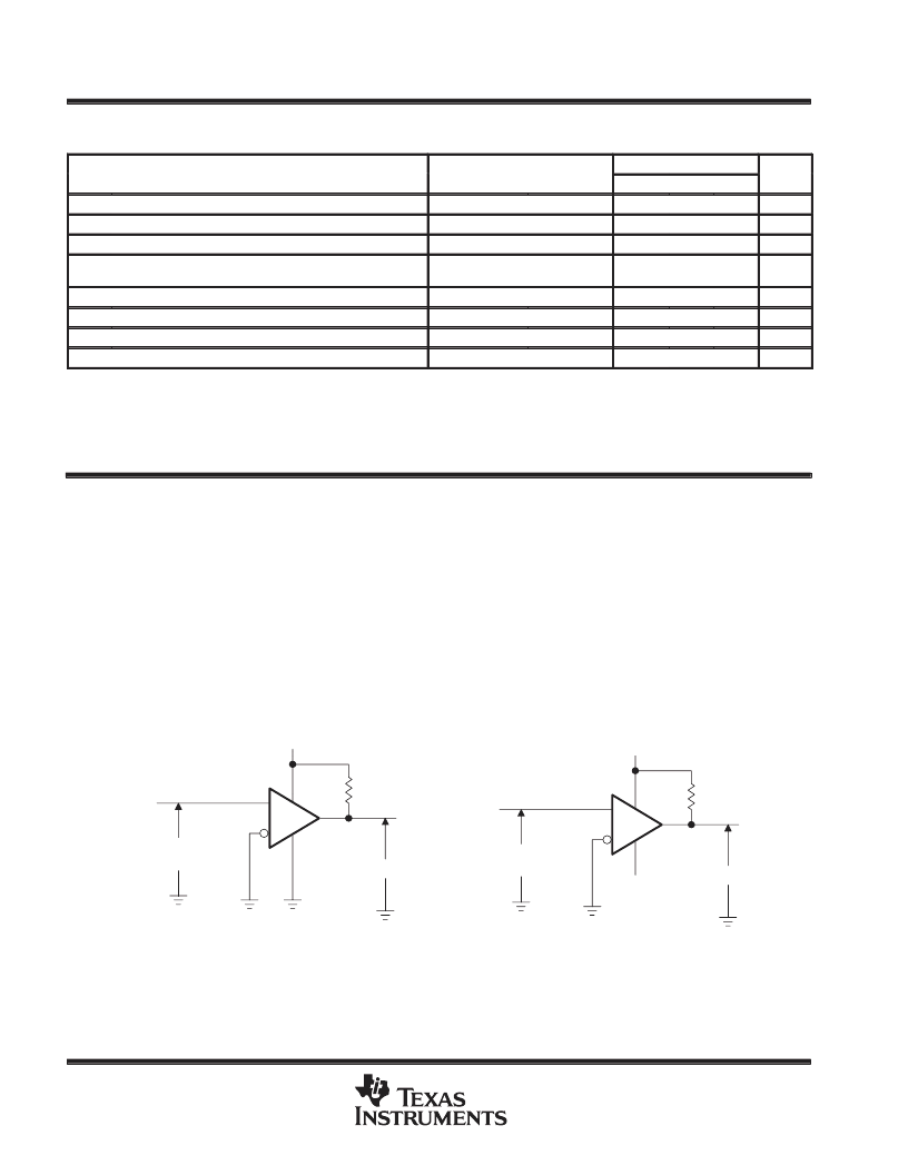
The digital output stage of the TLC372 can be damaged if it is held in the linear region of the transfer curve.
Conventional operational amplifier/comparator testing incorporates the use of a servo loop that is designed to force
the device output to a level within this linear region. Since the servo-loop method of testing cannot be used, the
following alternatives for measuring parameters such as input offset voltage, common-mode rejection, etc., are
offered.
To verify that the input offset voltage falls within the limits specified, the limit value is applied to the input as shown
in Figure 1(a). With the noninverting input positive with respect to the inverting input, the output should be high. With
the input polarity reversed, the output should be low.
A similar test can be made to verify the input offset voltage at the common-mode extremes. The supply voltages can
be slewed as shown in Figure 1(b) for the V
ICR
test, rather than changing the input voltages, to provide greater
accuracy.
5 V
5.1 k
VO
Applied VIO
Limit
VO
5.1 k
1 V
–4 V
–
+
–
+
(a) VIO WITH VIC = 0
(b) VIO WITH VIC = 4 V
Applied VIO
Limit
Figure 1. Method for Verifying That Input Offset Voltage is Within Specified Limits
相关PDF资料 |
PDF描述 |
|---|---|
| TLC374QD | LinCMOSE QUADRUPLE DIFFERENTIAL COMPARATORS |
| TLC374MFK | LinCMOSE QUADRUPLE DIFFERENTIAL COMPARATORS |
| TLC374MN | LinCMOSE QUADRUPLE DIFFERENTIAL COMPARATORS |
| TLC374Q | LinCMOSE QUADRUPLE DIFFERENTIAL COMPARATORS |
| TLC374QN | LinCMOSE QUADRUPLE DIFFERENTIAL COMPARATORS |
相关代理商/技术参数 |
参数描述 |
|---|---|
| TLC374 | 制造商:TI 制造商全称:Texas Instruments 功能描述:LinCMOSE QUADRUPLE DIFFERENTIAL COMPARATORS |
| TLC3741DR | 制造商:Texas Instruments 功能描述:- Tape and Reel |
| TLC374CD | 功能描述:校验器 IC Quad LiNCMOS RoHS:否 制造商:STMicroelectronics 产品: 比较器类型: 通道数量: 输出类型:Push-Pull 电源电压-最大:5.5 V 电源电压-最小:1.1 V 补偿电压(最大值):6 mV 电源电流(最大值):1350 nA 响应时间: 最大工作温度:+ 125 C 安装风格:SMD/SMT 封装 / 箱体:SC-70-5 封装:Reel |
| TLC374CDB | 制造商:Texas Instruments 功能描述:Comparator Quad |
| TLC374CDG4 | 功能描述:校验器 IC Quad LinCMOS Differential RoHS:否 制造商:STMicroelectronics 产品: 比较器类型: 通道数量: 输出类型:Push-Pull 电源电压-最大:5.5 V 电源电压-最小:1.1 V 补偿电压(最大值):6 mV 电源电流(最大值):1350 nA 响应时间: 最大工作温度:+ 125 C 安装风格:SMD/SMT 封装 / 箱体:SC-70-5 封装:Reel |
发布紧急采购,3分钟左右您将得到回复。