- 您现在的位置:买卖IC网 > PDF目录98239 > TLC4545IDR (TEXAS INSTRUMENTS INC) 1-CH 16-BIT SUCCESSIVE APPROXIMATION ADC, SERIAL ACCESS, PDSO8 PDF资料下载
参数资料
| 型号: | TLC4545IDR |
| 厂商: | TEXAS INSTRUMENTS INC |
| 元件分类: | ADC |
| 英文描述: | 1-CH 16-BIT SUCCESSIVE APPROXIMATION ADC, SERIAL ACCESS, PDSO8 |
| 封装: | GREEN, PLASTIC, MS-012AA, SOIC-8 |
| 文件页数: | 21/26页 |
| 文件大小: | 652K |
| 代理商: | TLC4545IDR |
TLC4541, TLC4545
SLAS293 DECEMBER 2001
4
www.ti.com
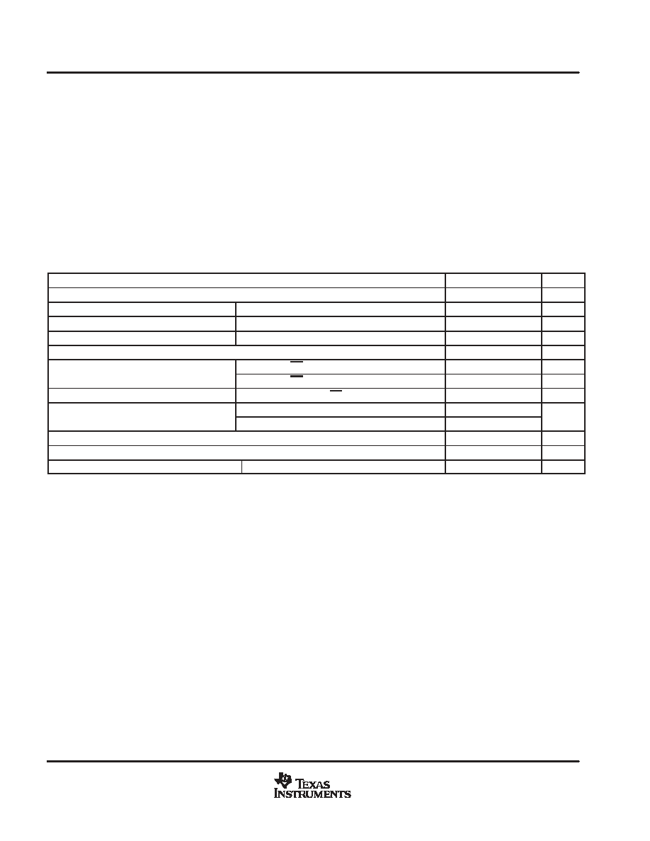
absolute maximum ratings over operating free-air temperature (unless otherwise noted)
Supply voltage, GND to VDD
0.3 V to 6.5V
. . . . . . . . . . . . . . . . . . . . . . . . . . . . . . . . . . . . . . . . . . . . . . . . . . . . . . . .
Analog input voltage range
0.3 V to VDD+0.3 V
. . . . . . . . . . . . . . . . . . . . . . . . . . . . . . . . . . . . . . . . . . . . . . . . . . . .
Reference input voltage
VDD+0.3 V
. . . . . . . . . . . . . . . . . . . . . . . . . . . . . . . . . . . . . . . . . . . . . . . . . . . . . . . . . . . . . . .
Digital input voltage range
0.3 V to VDD+0.3 V
. . . . . . . . . . . . . . . . . . . . . . . . . . . . . . . . . . . . . . . . . . . . . . . . . . . . .
Operating virtual junction temperature range, TJ
40
°C to 150°C
. . . . . . . . . . . . . . . . . . . . . . . . . . . . . . . . . . . . . .
Operating free-air temperature range: TA (I)
40
°C to 85°C
. . . . . . . . . . . . . . . . . . . . . . . . . . . . . . . . . . . . . . . . . .
Storage temperature range, Tstg
65
°C to 150°C
. . . . . . . . . . . . . . . . . . . . . . . . . . . . . . . . . . . . . . . . . . . . . . . . . . .
Lead temperature 1,6 mm (1/16 inch) from case for 10 seconds
260
°C
. . . . . . . . . . . . . . . . . . . . . . . . . . . . . . . .
Stresses beyond those listed under “absolute maximum ratings” may cause permanent damage to the device. These are stress ratings only, and
functional operation of the device at these or any other conditions beyond those indicated under “recommended operating conditions” is not
implied. Exposure to absolute-maximum-rated conditions for extended periods may affect device reliability.
recommended operating conditions
MIN
NOM
MAX
UNIT
Supply voltage, VDD
4.5
5
5.5
V
Frequency, SCLK
VDD = 2.7 V to 5.5 V
100
15000
kHz
Tolerable clock jitter, SCLK
VDD = 2.7 V to 5.5 V
24
ps
Aperature jitter
VDD = 2.7 V to 5.5 V
100
ps
External reference voltage input, VREF
4
VDD
V
VREF input impedance
VDD = 5 V, CS = 1, SCLK = 0
100
M
VREF input impedance
VDD = 5 V, CS = 0, SCLK = 15 MHz
20
25
k
External reference input current
VDD = VREF = 4.5 V, CS=0, SCLK = 15 MHz
0.02
1
mA
Analog input voltage
AIN, AIN(+)
0
VDD
V
Analog input voltage
AIN()
0.2
V
High level control input voltage, VIH
2.1
V
Low level control input voltage, VIL
0.8
V
Operating free-air temperature, TA
TLC4541/45I
40
85
°C
相关PDF资料 |
PDF描述 |
|---|---|
| TLC4541IDGKG4 | 1-CH 16-BIT SUCCESSIVE APPROXIMATION ADC, SERIAL ACCESS, PDSO8 |
| TLC4541ID | 1-CH 16-BIT SUCCESSIVE APPROXIMATION ADC, SERIAL ACCESS, PDSO8 |
| TLC4541IDGKRG4 | 1-CH 16-BIT SUCCESSIVE APPROXIMATION ADC, SERIAL ACCESS, PDSO8 |
| TLC4545IDGKR | 1-CH 16-BIT SUCCESSIVE APPROXIMATION ADC, SERIAL ACCESS, PDSO8 |
| TLC4541IDGKR | 1-CH 16-BIT SUCCESSIVE APPROXIMATION ADC, SERIAL ACCESS, PDSO8 |
相关代理商/技术参数 |
参数描述 |
|---|---|
| TLC4545IDRG4 | 功能描述:模数转换器 - ADC 16-Bit 200KSPS Serial Out RoHS:否 制造商:Texas Instruments 通道数量:2 结构:Sigma-Delta 转换速率:125 SPs to 8 KSPs 分辨率:24 bit 输入类型:Differential 信噪比:107 dB 接口类型:SPI 工作电源电压:1.7 V to 3.6 V, 2.7 V to 5.25 V 最大工作温度:+ 85 C 安装风格:SMD/SMT 封装 / 箱体:VQFN-32 |
| TLC-4C-0375 | 制造商:KATO/COILTHREAD 功能描述: |
| TLC-4C-0375W | 制造商:KATO/COILTHREAD 功能描述: |
| TLC-4C-0500 | 制造商:KATO/COILTHREAD 功能描述: |
| TL-C5-140-30 | 制造商:Newport Electronics Inc 功能描述:5-DOT ROUND LABELS |
发布紧急采购,3分钟左右您将得到回复。