- 您现在的位置:买卖IC网 > PDF目录98239 > TLC4545IDR (TEXAS INSTRUMENTS INC) 1-CH 16-BIT SUCCESSIVE APPROXIMATION ADC, SERIAL ACCESS, PDSO8 PDF资料下载
参数资料
| 型号: | TLC4545IDR |
| 厂商: | TEXAS INSTRUMENTS INC |
| 元件分类: | ADC |
| 英文描述: | 1-CH 16-BIT SUCCESSIVE APPROXIMATION ADC, SERIAL ACCESS, PDSO8 |
| 封装: | GREEN, PLASTIC, MS-012AA, SOIC-8 |
| 文件页数: | 22/26页 |
| 文件大小: | 652K |
| 代理商: | TLC4545IDR |
TLC4541, TLC4545
SLAS293 DECEMBER 2001
5
www.ti.com
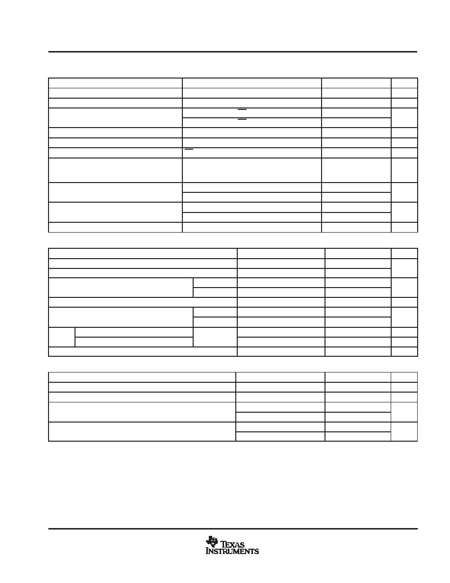
electrical characteristics over recommended operating free-air temperature range,
VDD = 5 V, VREF = 4.096 V, SCLK frequency = 15 MHz (unless otherwise noted)
PARAMETER
TEST CONDITIONS
MIN
TYP
MAX
UNIT
VOH
High-level output voltage
VDD = 4.5 V,
IOH = 0.2 mA
3.9
V
VOL
Low-level output voltage
VDD = 4.5 V,
IOL = 0.8 mA
0.4
V
IOZ
Off-state output current
VO = VDD,
CS = VDD
1
2.5
A
IOZ
Off-state output current
(high-impedance-state)
VO = 0,
CS = VDD
1
2.5
A
IIH
High-level input current
VI = VDD
0.005
2.5
A
IIL
Low-level input current
VI = 0
0.005
2.5
A
ICC
Operating supply current
CS at 0 V,
VDD = 4.5 V to 5.5 V
3.5
mA
ICC(PD) Power-down supply current
For all digital inputs, 0
≤ VI ≤ 0.3 V or
VI ≥ VDD 0.3 V, SCLK=VDD,
VDD = 4.5 V to 5.5 V
3
5
A
Selected analog input channel
Selected channel at VDD
1
A
Selected analog input channel
leakage current
Selected channel at 0 V
1
A
Ci
Input capacitance
Analog inputs
11
14
pF
Ci
Input capacitance
Control Inputs
20
25
pF
Zi
Input resistance
VDD = 5.5 V
500
ac specifications (TLC4541/45)
PARAMETER
TEST CONDITIONS
MIN
TYP
MAX
UNIT
SINAD
Signal-to-noise ratio + distortion
fI = 15 kHz at 200 KSPS
84.5
dB
SNR
Signal-to-noise ratio
fI = 15 kHz at 200 KSPS
85
dB
THD
Total harmonic distortion
TLC4541
fI = 15 kHz at 200 KSPS
94
87
dB
THD
Total harmonic distortion
TLC4545
fI = 15 kHz at 200 KSPS
94
89
dB
ENOB
Effective number of bits
fI = 15 kHz at 200 KSPS
13.7
Bits
SFDR
Spurious free dynamic range
TLC4541
fI = 15 kHz at 200 KSPS
95
87
dB
SFDR
Spurious free dynamic range
TLC4545
fI = 15 kHz at 200 KSPS
95
89
dB
Full power bandwidth, 3 dB, analog input
1
MHz
Full power bandwidth, 1 dB, analog input
500
kHz
Crosstalk
0.25 LBS
80
dB
dc specifications (TLC4541/45)
PARAMETER
TEST CONDITIONS
MIN
TYP
MAX
UNIT
INL
Integral linearity error (see Note 1)
2.5
LSB
DNL
Differential linearity error
1
2
LSB
EO
Offset error (see Note 2)
TLC4541
3.5
mV
EO
Offset error (see Note 2)
TLC4545
1
mV
EG
Gain error (see Note 2)
TLC4541
2
mV
EG
Gain error (see Note 2)
TLC4545
1.8
mV
All typical values are at VDD = 5 V, TA = 25°C.
NOTES:
1. Linear error is the maximum deviation from the best straight line through the A/D transfer characteristics.
2. Zero error is the difference between 0000h and the converted output for zero input voltage: full-scale error is the difference between
ideal full-scale and the converted output for full-scale input voltage.
相关PDF资料 |
PDF描述 |
|---|---|
| TLC4541IDGKG4 | 1-CH 16-BIT SUCCESSIVE APPROXIMATION ADC, SERIAL ACCESS, PDSO8 |
| TLC4541ID | 1-CH 16-BIT SUCCESSIVE APPROXIMATION ADC, SERIAL ACCESS, PDSO8 |
| TLC4541IDGKRG4 | 1-CH 16-BIT SUCCESSIVE APPROXIMATION ADC, SERIAL ACCESS, PDSO8 |
| TLC4545IDGKR | 1-CH 16-BIT SUCCESSIVE APPROXIMATION ADC, SERIAL ACCESS, PDSO8 |
| TLC4541IDGKR | 1-CH 16-BIT SUCCESSIVE APPROXIMATION ADC, SERIAL ACCESS, PDSO8 |
相关代理商/技术参数 |
参数描述 |
|---|---|
| TLC4545IDRG4 | 功能描述:模数转换器 - ADC 16-Bit 200KSPS Serial Out RoHS:否 制造商:Texas Instruments 通道数量:2 结构:Sigma-Delta 转换速率:125 SPs to 8 KSPs 分辨率:24 bit 输入类型:Differential 信噪比:107 dB 接口类型:SPI 工作电源电压:1.7 V to 3.6 V, 2.7 V to 5.25 V 最大工作温度:+ 85 C 安装风格:SMD/SMT 封装 / 箱体:VQFN-32 |
| TLC-4C-0375 | 制造商:KATO/COILTHREAD 功能描述: |
| TLC-4C-0375W | 制造商:KATO/COILTHREAD 功能描述: |
| TLC-4C-0500 | 制造商:KATO/COILTHREAD 功能描述: |
| TL-C5-140-30 | 制造商:Newport Electronics Inc 功能描述:5-DOT ROUND LABELS |
发布紧急采购,3分钟左右您将得到回复。