- 您现在的位置:买卖IC网 > PDF目录69494 > TLE8242 (INFINEON TECHNOLOGIES AG) SPECIALTY ANALOG CIRCUIT, PQFP64 PDF资料下载
参数资料
| 型号: | TLE8242 |
| 厂商: | INFINEON TECHNOLOGIES AG |
| 元件分类: | 模拟信号调理 |
| 英文描述: | SPECIALTY ANALOG CIRCUIT, PQFP64 |
| 封装: | GREEN, PLASTIC, LQFP-64 |
| 文件页数: | 10/77页 |
| 文件大小: | 1580K |
| 代理商: | TLE8242 |
第1页第2页第3页第4页第5页第6页第7页第8页第9页当前第10页第11页第12页第13页第14页第15页第16页第17页第18页第19页第20页第21页第22页第23页第24页第25页第26页第27页第28页第29页第30页第31页第32页第33页第34页第35页第36页第37页第38页第39页第40页第41页第42页第43页第44页第45页第46页第47页第48页第49页第50页第51页第52页第53页第54页第55页第56页第57页第58页第59页第60页第61页第62页第63页第64页第65页第66页第67页第68页第69页第70页第71页第72页第73页第74页第75页第76页第77页
TLE8242
Functional Description and Electrical Characteristics
Data Sheet
18
Rev. 1.0, 2009-02-25
5.2
Input / Output
All digital inputs are compatible with 3.3 V and 5 V I/O logic levels. The supply voltage for the SPI output SO is the
V_SIGNAL pin. All digital inputs are pulled to a known state by a weak internal current source or current sink when
not connected. However, unused digital input pins should be connected to ground or to V_SIGNAL (according to
the desired functionality) by an external connection or resistor. All input pin weak internal current sources are
supplied by the V_SIGNAL pin.
The RESET_B pin is an active low input pin. When this pin is low, all channels are off, and all internal registers
are reset to their default states. The device must be held in reset by an external source until all the power supplies
have stabilized. The IC contains an internal power on and undervoltage reset which becomes active when V5D,
V5A1, V5A2, or V5A3 fall below the undervoltage reset thresholds.
The ENABLE pin is an active high input pin which must be held high for normal operation of the device. When this
pin is held low all channels are either turned off or will remain in the last state, depending on how the enable
behavior of the channel is programmed via SPI Message #10. The default condition is that all channels are turned
off when the ENABLE pin is low.
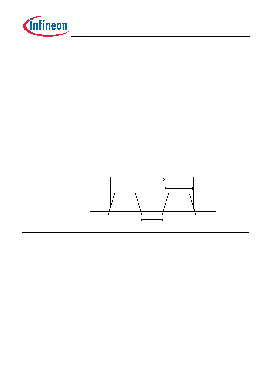
The CLK pin is the main clock input for the device. The input thresholds are compatible with 3.3 V and 5.0 V logic
levels. No synchronization is required between the clock signal connected to the CLK pin and the SPI clock signal
(SCK). All internal clock signals of the TLE8242 (PWM signals, A/D sampling, diagnostics, etc.) are generated
from the this clock input. Also, this clock is required for the device to accept and respond to SPI messages.
Figure 7
CLK Timing Diagram
The PHASE_SYNC pin is an input pin that can be used by the microcontroller to synchronize the PWM control
signals of multiple channels. The desired phase delay between the rising edge of the signal applied to the
PHASE_SYNC pin and the rising edge of the PWM signal of each channel can be programmed independently via
SPI message #6. The equation for calculating the offset is:
Each time a pulse is received on the PHASE_SYNC pin, the IC will latch a bit which is reported via the response
to SPI message #19. (See SPI interface section for bit/message location.) This latch is cleared when the message
is read.
Note: The PWM periods are restarted when a rising edge is detected on the PHASE_SYNC pin. A periodic pulse
train on this pin will disturb the current regulation.
CLK
t
14
1/f
clk
t
15
VIH
min
VIL
max
PWM
offset
F
Offset
PhaseSynch
T
*
32
=
相关PDF资料 |
PDF描述 |
|---|---|
| TLE8386EL | 0.09 A SWITCHING CONTROLLER, 500 kHz SWITCHING FREQ-MAX, PDSO14 |
| TLI4946-2L | MAGNETIC SENSOR, PSIP3 |
| TLI4946K | MAGNETIC SENSOR, PDSO3 |
| TLV431AIDBVR | 1-OUTPUT THREE TERM VOLTAGE REFERENCE, 1.24 V, PDSO5 |
| TLV431ACDBVT | 1-OUTPUT THREE TERM VOLTAGE REFERENCE, 1.24 V, PDSO5 |
相关代理商/技术参数 |
参数描述 |
|---|---|
| TLE8242-2 | 制造商:INFINEON 制造商全称:Infineon Technologies AG 功能描述:8 Channel Fixed Frequency Constant Current Control With Current Profile Detection |
| TLE82452SAALLA1 | 制造商:Infineon Technologies AG 功能描述:TRANSMISSION_IC - Rail/Tube |
| TLE82452SAAUMA1 | 制造商:Infineon Technologies AG 功能描述:TRANSMISSION_IC - Tape and Reel |
| TLE8250G | 功能描述:CAN 接口集成电路 High Speed CAN Transceiver RoHS:否 制造商:Texas Instruments 类型:Transceivers 工作电源电压:5 V 电源电流: 工作温度范围:- 40 C to + 85 C 封装 / 箱体:SOIC-8 封装:Tube |
| TLE8250GVIO | 功能描述:CAN 接口集成电路 High Speed CAN Transceiver RoHS:否 制造商:Texas Instruments 类型:Transceivers 工作电源电压:5 V 电源电流: 工作温度范围:- 40 C to + 85 C 封装 / 箱体:SOIC-8 封装:Tube |
发布紧急采购,3分钟左右您将得到回复。