- 您现在的位置:买卖IC网 > PDF目录98249 > TLV1549IDG4 (TEXAS INSTRUMENTS INC) 1-CH 10-BIT SUCCESSIVE APPROXIMATION ADC, SERIAL ACCESS, PDSO8 PDF资料下载
参数资料
| 型号: | TLV1549IDG4 |
| 厂商: | TEXAS INSTRUMENTS INC |
| 元件分类: | ADC |
| 英文描述: | 1-CH 10-BIT SUCCESSIVE APPROXIMATION ADC, SERIAL ACCESS, PDSO8 |
| 封装: | GREEN, SOIC-8 |
| 文件页数: | 13/19页 |
| 文件大小: | 429K |
| 代理商: | TLV1549IDG4 |
TLV1549C, TLV1549I, TLV1549M
10-BIT ANALOG-TO-DIGITAL CONVERTERS
WITH SERIAL CONTROL
SLAS071C – JANUARY 1993 – REVISED MARCH 1995
3
POST OFFICE BOX 655303
DALLAS, TEXAS 75265
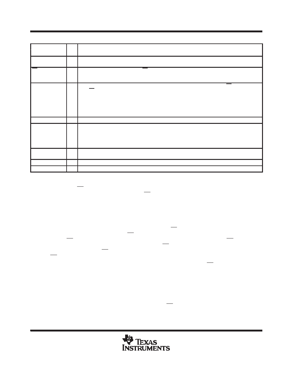
Terminal Functions
TERMINAL
I/O
DESCRIPTION
NAME
NO.
I/O
DESCRIPTION
ANALOG IN
2
I
Analog input. The driving source impedance should be
≤ 1 kΩ. The external driving source to ANALOG IN should
have a current capability
≥ 10 mA.
CS
5
I
Chip select. A high-to-low transition on CS resets the internal counters and controls and enables DATA OUT and
I/O CLOCK within a maximum of a setup time plus two falling edges of the internal system clock. A low-to-high
transition disables I/O CLOCK within a setup time plus two falling edges of the internal system clock.
DATA OUT
6
O
This 3-state serial output for the A/D conversion result is in the high-impedance state when CS is high and active
when CS is low. With a valid chip select, DATA OUT is removed from the high-impedance state and is driven to
the logic level corresponding to the MSB value of the previous conversion result. The next falling edge of I/O
CLOCK drives DATA OUT to the logic level corresponding to the next most significant bit, and the remaining bits
are shifted out in order with the LSB appearing on the ninth falling edge of I/O CLOCK. On the tenth falling edge
of I/O CLOCK, DATA OUT is driven to a low logic level so that serial interface data transfers of more than ten clocks
produce zeroes as the unused LSBs.
GND
4
I
The ground return for internal circuitry. Unless otherwise noted, all voltage measurements are with respect to GND.
I/O CLOCK
7
I
The input /output clock receives the serial I/O CLOCK input and performs the following three functions:
1) On the third falling edge of I/O CLOCK, the analog input voltage begins charging the capacitor array and
continues to do so until the tenth falling edge of I/O CLOCK.
2) It shifts the nine remaining bits of the previous conversion data out on DATA OUT.
3) It transfers control of the conversion to the internal state controller on the falling edge of the tenth clock.
REF +
1
I
The upper reference voltage value (nominally VCC) is applied to REF+. The maximum input voltage range is
determined by the difference between the voltage applied to REF + and the voltage applied to REF –.
REF –
3
I
The lower reference voltage value (nominally ground) is applied to this REF –.
VCC
8
I
Positive supply voltage
detailed description
With chip select (CS) inactive (high), the I/O CLOCK input is initially disabled and DATA OUT is in the high-
impedance state. When the serial interface takes CS active (low), the conversion sequence begins with the
enabling of I/O CLOCK and the removal of DATA OUT from the high-impedance state. The serial interface then
provides the I/O CLOCK sequence to I/O CLOCK and receives the previous conversion result from DATA OUT.
I/O CLOCK receives an input sequence that is between 10 and 16 clocks long from the host serial interface.
The first ten I/O clocks provide the control timing for sampling the analog input.
There are six basic serial interface timing modes that can be used with the TLV1549. These modes are
determined by the speed of I/O CLOCK and the operation of CS as shown in Table 1. These modes are:
(1) a fast mode with a 10-clock transfer and CS inactive (high) between transfers, (2) a fast mode with a 10-clock
transfer and CS active (low) continuously, (3) a fast mode with an 11- to 16-clock transfer and CS inactive (high)
between transfers, (4) a fast mode with a 16-bit transfer and CS active (low) continuously, (5) a slow mode with
an 11- to 16-clock transfer and CS inactive (high) between transfers, and (6) a slow mode with a 16-clock transfer
and CS active (low) continuously.
The MSB of the previous conversion appears on DATA OUT on the falling edge of CS in mode 1, mode 3, and
mode 5, within 21
μs from the falling edge of the tenth I/O CLOCK in mode 2 and mode 4, and following the
16th clock falling edge in mode 6. The remaining nine bits are shifted out on the next nine falling edges of the
I/O CLOCK. Ten bits of data are transmitted to the host serial interface through DATA OUT. The number of serial
clock pulses used also depends on the mode of operation, but a minimum of ten clock pulses is required for
conversion to begin. On the tenth clock falling edge, the internal logic takes DATA OUT low to ensure that the
remaining bit values are zero if the I/O CLOCK transfer is more than ten clocks long.
Table 1 lists the operational modes with respect to the state of CS, the number of I/O serial transfer clocks that
can be used, and the timing on which the MSB of the previous conversion appears at the output.
相关PDF资料 |
PDF描述 |
|---|---|
| TLV1549ID | 1-CH 10-BIT SUCCESSIVE APPROXIMATION ADC, SERIAL ACCESS, PDSO8 |
| TLV1549CD | 1-CH 10-BIT SUCCESSIVE APPROXIMATION ADC, SERIAL ACCESS, PDSO8 |
| TLV1562CDWRG4 | 4-CH 10-BIT PROPRIETARY METHOD ADC, PARALLEL ACCESS, PDSO28 |
| TLV1562CDWG4 | 4-CH 10-BIT PROPRIETARY METHOD ADC, PARALLEL ACCESS, PDSO28 |
| TLV1562CDWR | 4-CH 10-BIT PROPRIETARY METHOD ADC, PARALLEL ACCESS, PDSO28 |
相关代理商/技术参数 |
参数描述 |
|---|---|
| TLV1549IDR | 功能描述:模数转换器 - ADC 10B 38kSPS Ser Out Inherent S&H Fctn RoHS:否 制造商:Texas Instruments 通道数量:2 结构:Sigma-Delta 转换速率:125 SPs to 8 KSPs 分辨率:24 bit 输入类型:Differential 信噪比:107 dB 接口类型:SPI 工作电源电压:1.7 V to 3.6 V, 2.7 V to 5.25 V 最大工作温度:+ 85 C 安装风格:SMD/SMT 封装 / 箱体:VQFN-32 |
| TLV1549IDRG4 | 功能描述:模数转换器 - ADC 10B 38kSPS Ser Out Inherent S&H Fctn RoHS:否 制造商:Texas Instruments 通道数量:2 结构:Sigma-Delta 转换速率:125 SPs to 8 KSPs 分辨率:24 bit 输入类型:Differential 信噪比:107 dB 接口类型:SPI 工作电源电压:1.7 V to 3.6 V, 2.7 V to 5.25 V 最大工作温度:+ 85 C 安装风格:SMD/SMT 封装 / 箱体:VQFN-32 |
| TLV1549IP | 功能描述:模数转换器 - ADC Single Serial In RoHS:否 制造商:Texas Instruments 通道数量:2 结构:Sigma-Delta 转换速率:125 SPs to 8 KSPs 分辨率:24 bit 输入类型:Differential 信噪比:107 dB 接口类型:SPI 工作电源电压:1.7 V to 3.6 V, 2.7 V to 5.25 V 最大工作温度:+ 85 C 安装风格:SMD/SMT 封装 / 箱体:VQFN-32 |
| TLV1549IPE4 | 功能描述:模数转换器 - ADC 10-Bit 38 kSPS Serial Out RoHS:否 制造商:Texas Instruments 通道数量:2 结构:Sigma-Delta 转换速率:125 SPs to 8 KSPs 分辨率:24 bit 输入类型:Differential 信噪比:107 dB 接口类型:SPI 工作电源电压:1.7 V to 3.6 V, 2.7 V to 5.25 V 最大工作温度:+ 85 C 安装风格:SMD/SMT 封装 / 箱体:VQFN-32 |
| TLV1549M | 制造商:TI 制造商全称:Texas Instruments 功能描述:10-BIT ANALOG-TO-DIGITAL CONVERTERS WITH SERIAL CONTROL |
发布紧急采购,3分钟左右您将得到回复。