- 您现在的位置:买卖IC网 > PDF目录98249 > TLV1549IDG4 (TEXAS INSTRUMENTS INC) 1-CH 10-BIT SUCCESSIVE APPROXIMATION ADC, SERIAL ACCESS, PDSO8 PDF资料下载
参数资料
| 型号: | TLV1549IDG4 |
| 厂商: | TEXAS INSTRUMENTS INC |
| 元件分类: | ADC |
| 英文描述: | 1-CH 10-BIT SUCCESSIVE APPROXIMATION ADC, SERIAL ACCESS, PDSO8 |
| 封装: | GREEN, SOIC-8 |
| 文件页数: | 19/19页 |
| 文件大小: | 429K |
| 代理商: | TLV1549IDG4 |
TLV1549C, TLV1549I, TLV1549M
10-BIT ANALOG-TO-DIGITAL CONVERTERS
WITH SERIAL CONTROL
SLAS071C – JANUARY 1993 – REVISED MARCH 1995
9
POST OFFICE BOX 655303
DALLAS, TEXAS 75265
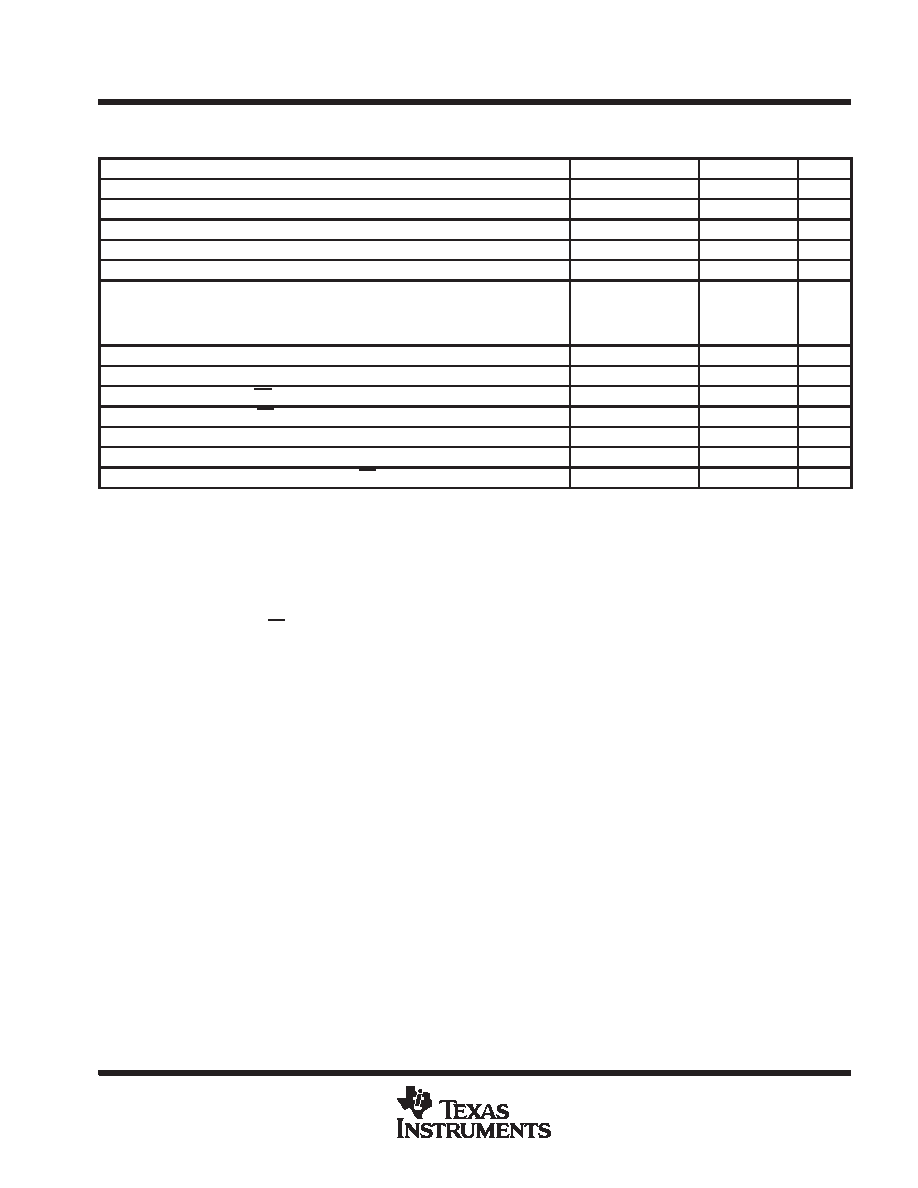
operating characteristics over recommended operating free-air temperature range,
VCC = Vref+ = 3 V to 3.6 V, I/O CLOCK frequency = 2.1 MHz
PARAMETER
TEST CONDITIONS
MIN
MAX
UNIT
Linearity error (see Note 6)
±1
LSB
Zero error (see Note 7)
See Note 2
±1
LSB
Full-scale error (see Note 7)
See Note 2
±1
LSB
Total unadjusted error (see Note 8)
±1
LSB
tconv
Conversion time
See Figures 6 – 11
21
μs
tc
Total cycle time (access, sample, and conversion)
See Figures 6 – 11
and Note 9
21
+ 10 I/O
CLOCK
periods
μs
tv
Valid time, DATA OUT remains valid after I/O CLOCK
↓
See Figure 5
10
ns
td(I/O-DATA) Delay time, I/O CLOCK↓ to DATA OUT valid
See Figure 5
240
ns
tPZH, tPZL
Enable time, CS
↓ to DATA OUT (MSB driven)
See Figure 3
1.3
μs
tPHZ, tPLZ
Disable time, CS
↑ to DATA OUT (high impedance)
See Figure 3
180
ns
tr(bus)
Rise time, data bus
See Figure 5
300
ns
tf(bus)
Fall time, data bus
See Figure 5
300
ns
td(I/O-CS)
Delay time, 10th I/O CLOCK
↓ to CS↓ to abort conversion (see Note10)
9
μs
NOTES: 2. Analog input voltages greater than that applied to REF + convert as all ones (1111111111), while input voltages less than that applied
to REF – convert as all zeros (0000000000). The device is functional with reference voltages down to 1 V (Vref+ – Vref–); however,
the electrical specifications are no longer applicable.
6. Linearity error is the maximum deviation from the best straight line through the A / D transfer characteristics.
7. Zero error is the difference between 0000000000 and the converted output for zero input voltage; full-scale error is the difference
between 1111111111 and the converted output for full-scale input voltage.
8. Total unadjusted error comprises linearity, zero, and full-scale errors.
9. I/O CLOCK period = 1/(I/O CLOCK frequency). Sampling begins on the falling edge of the third I/O CLOCK, continues for seven
I/O CLOCK periods, and ends on the falling edge of the tenth I/O CLOCK (see Figure 5).
10. Any transitions of CS are recognized as valid only if the level is maintained for a minimum of a setup time plus two falling edges of
the internal clock (1.425
μs) after the transition.
相关PDF资料 |
PDF描述 |
|---|---|
| TLV1549ID | 1-CH 10-BIT SUCCESSIVE APPROXIMATION ADC, SERIAL ACCESS, PDSO8 |
| TLV1549CD | 1-CH 10-BIT SUCCESSIVE APPROXIMATION ADC, SERIAL ACCESS, PDSO8 |
| TLV1562CDWRG4 | 4-CH 10-BIT PROPRIETARY METHOD ADC, PARALLEL ACCESS, PDSO28 |
| TLV1562CDWG4 | 4-CH 10-BIT PROPRIETARY METHOD ADC, PARALLEL ACCESS, PDSO28 |
| TLV1562CDWR | 4-CH 10-BIT PROPRIETARY METHOD ADC, PARALLEL ACCESS, PDSO28 |
相关代理商/技术参数 |
参数描述 |
|---|---|
| TLV1549IDR | 功能描述:模数转换器 - ADC 10B 38kSPS Ser Out Inherent S&H Fctn RoHS:否 制造商:Texas Instruments 通道数量:2 结构:Sigma-Delta 转换速率:125 SPs to 8 KSPs 分辨率:24 bit 输入类型:Differential 信噪比:107 dB 接口类型:SPI 工作电源电压:1.7 V to 3.6 V, 2.7 V to 5.25 V 最大工作温度:+ 85 C 安装风格:SMD/SMT 封装 / 箱体:VQFN-32 |
| TLV1549IDRG4 | 功能描述:模数转换器 - ADC 10B 38kSPS Ser Out Inherent S&H Fctn RoHS:否 制造商:Texas Instruments 通道数量:2 结构:Sigma-Delta 转换速率:125 SPs to 8 KSPs 分辨率:24 bit 输入类型:Differential 信噪比:107 dB 接口类型:SPI 工作电源电压:1.7 V to 3.6 V, 2.7 V to 5.25 V 最大工作温度:+ 85 C 安装风格:SMD/SMT 封装 / 箱体:VQFN-32 |
| TLV1549IP | 功能描述:模数转换器 - ADC Single Serial In RoHS:否 制造商:Texas Instruments 通道数量:2 结构:Sigma-Delta 转换速率:125 SPs to 8 KSPs 分辨率:24 bit 输入类型:Differential 信噪比:107 dB 接口类型:SPI 工作电源电压:1.7 V to 3.6 V, 2.7 V to 5.25 V 最大工作温度:+ 85 C 安装风格:SMD/SMT 封装 / 箱体:VQFN-32 |
| TLV1549IPE4 | 功能描述:模数转换器 - ADC 10-Bit 38 kSPS Serial Out RoHS:否 制造商:Texas Instruments 通道数量:2 结构:Sigma-Delta 转换速率:125 SPs to 8 KSPs 分辨率:24 bit 输入类型:Differential 信噪比:107 dB 接口类型:SPI 工作电源电压:1.7 V to 3.6 V, 2.7 V to 5.25 V 最大工作温度:+ 85 C 安装风格:SMD/SMT 封装 / 箱体:VQFN-32 |
| TLV1549M | 制造商:TI 制造商全称:Texas Instruments 功能描述:10-BIT ANALOG-TO-DIGITAL CONVERTERS WITH SERIAL CONTROL |
发布紧急采购,3分钟左右您将得到回复。