- 您现在的位置:买卖IC网 > PDF目录98249 > TLV1562CDW (TEXAS INSTRUMENTS INC) 4-CH 10-BIT PROPRIETARY METHOD ADC, PARALLEL ACCESS, PDSO28 PDF资料下载
参数资料
| 型号: | TLV1562CDW |
| 厂商: | TEXAS INSTRUMENTS INC |
| 元件分类: | ADC |
| 英文描述: | 4-CH 10-BIT PROPRIETARY METHOD ADC, PARALLEL ACCESS, PDSO28 |
| 封装: | 1.27 MM PITCH, SOIC-28 |
| 文件页数: | 34/41页 |
| 文件大小: | 600K |
| 代理商: | TLV1562CDW |
第1页第2页第3页第4页第5页第6页第7页第8页第9页第10页第11页第12页第13页第14页第15页第16页第17页第18页第19页第20页第21页第22页第23页第24页第25页第26页第27页第28页第29页第30页第31页第32页第33页当前第34页第35页第36页第37页第38页第39页第40页第41页
TLV1562
2.7 V TO 5.5 V, HIGH-SPEED LOW-POWER RECONFIGURABLE ANALOG-TO-DIGITAL
CONVERTER WITH 4-INPUT, DUAL S/H, PARALLEL INTERFACE, AND POWER DOWN
SLAS162 – SEPTEMBER 1998
4
POST OFFICE BOX 655303
DALLAS, TEXAS 75265
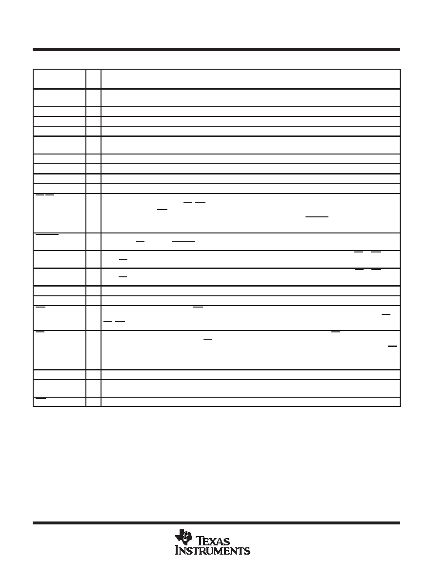
Terminal Functions
TERMINAL
I/O
DESCRIPTION
NAME
NO.
I/O
DESCRIPTION
AGND
20
I
Analog ground return for the internal circuitry. Unless otherwise noted, all analog voltage measurements are with
respect to AGND.
AM/CH2
26
I
Differential channel A input minus or single-ended channel 2
AP/CH1
27
I
Differential channel A input plus or single-ended channel 1
AVDD
23
I
Positive analog supply voltage
BDGND
8
I
Digital ground return for the I/O buffers. Unless otherwise noted, all digital interface voltage measurements are with
respect to DGND.
BDVDD
7
I
Positive digital supply voltage for I/O buffers
BM/CH4
24
I
Differential channel B input minus or single-ended channel 4
BP/CH3
25
I
Differential channel B input plus or single-ended channel 3
CLKIN
16
I
External clock input. (1 MHz to 15 MHz)
CS/OE
15
I
Chip select. A high-to-low transition on this input resets the internal counters and controls and enables the output data
bus D(0–9) and control inputs (RD, WR) within a maximum setup time. A low-to-high transition disables the output
data bus D(9–0) and WR within a maximum setup time. This signal also serves as an output enable signal when the
device is programmed into both mono and dual interrupt-driven modes using CSTART as the start of conversion
signal.
CSTART
1
I
Conversion start signal. A falling edge starts the sampling period and a rising edge starts the conversion. This signal
acts without CS activated. CSTART connects to DVDD via a 10-k pull-up resistor if not used.
D(0–4)
2–6
I/O
The lower bits of the 3-state parallel data bus. Bidirectional. The data bus is 3-stated except when RD or WR is low
when CS is low.
D(5–9)
9–13
I/O
The higher bits of the 3-state parallel data bus. Bidirectional. The data bus is 3-stated except when RD or WR is low
when CS is low. When the host processor writes to the converter, D(9,8) are used as an index to the internal registers.
DGND
18
I
Digital ground return for the internal digital logic circuitry
DVDD
17
I
Positive digital supply voltage
INT
14
O
Interrupt output. The falling edge of INT signals the end of conversion. This output goes from a high impedance state
to low logic level on the fifth falling edge of the system clock and remains low until reset by the rising edge of CS or
RD. INT requires connection of a 10-k
pull-up resistor.
RD
28
I
Processor read strobe or synchronous start of conversion/sampling. The falling edge of RD is used to 1) start the
conversion in interrupt-driven mode (if RD is programmed as the start conversion signal); 2) start both conversion
and next sampling plus release of the previous conversion data in both continuous modes. The rising edge of RD
serves as a read strobe and data is 3-stated (approximately 10 ns at 50 pF bus loading) after this edge. Connection
of a 10-k
pull-up resistor is optional.
VREFM
21
I
The lower voltage reference value is applied to this terminal.
VREFP
22
I
The upper reference voltage value is applied to this terminal. The maximum input voltage range is determined by the
difference between the voltage applied to this terminal and the VREFM terminal.
WR
19
I
Processor write strobe. Active low. Connection of a 10-k
pull-up resistor is optional.
detailed description
The TLV1562 analog-to-digital converter is based on an advanced low power recyclic architecture. Two bits of
the conversion result are presented per system clock cycle. A total of 5 system clock (SYSCLK) cycles is
required to complete the conversion. The serial conversion results are converted to a parallel word for output.
The device supports both interrupt-driven (typically found in a SAR type ADC) and continuous (natural for a
pipeline type ADC) modes of conversion. An innovative conversion scheme makes this device perfect for power
sensitive applications with uncompromised speed.
相关PDF资料 |
PDF描述 |
|---|---|
| TLV1562IDWR | 4-CH 10-BIT PROPRIETARY METHOD ADC, PARALLEL ACCESS, PDSO28 |
| TLV1562CPWR | 4-CH 10-BIT PROPRIETARY METHOD ADC, PARALLEL ACCESS, PDSO28 |
| TLV1562CPW | 4-CH 10-BIT PROPRIETARY METHOD ADC, PARALLEL ACCESS, PDSO28 |
| TLV1562IPWR | 4-CH 10-BIT PROPRIETARY METHOD ADC, PARALLEL ACCESS, PDSO28 |
| TLV1562IPW | 4-CH 10-BIT PROPRIETARY METHOD ADC, PARALLEL ACCESS, PDSO28 |
相关代理商/技术参数 |
参数描述 |
|---|---|
| TLV1562CDWR | 制造商:Rochester Electronics LLC 功能描述:- Bulk |
| TLV1562CPW | 功能描述:模数转换器 - ADC 10bit Programmable RoHS:否 制造商:Texas Instruments 通道数量:2 结构:Sigma-Delta 转换速率:125 SPs to 8 KSPs 分辨率:24 bit 输入类型:Differential 信噪比:107 dB 接口类型:SPI 工作电源电压:1.7 V to 3.6 V, 2.7 V to 5.25 V 最大工作温度:+ 85 C 安装风格:SMD/SMT 封装 / 箱体:VQFN-32 |
| TLV1562CPWG4 | 功能描述:模数转换器 - ADC 10-Bit 2 MSPS Quad Channel RoHS:否 制造商:Texas Instruments 通道数量:2 结构:Sigma-Delta 转换速率:125 SPs to 8 KSPs 分辨率:24 bit 输入类型:Differential 信噪比:107 dB 接口类型:SPI 工作电源电压:1.7 V to 3.6 V, 2.7 V to 5.25 V 最大工作温度:+ 85 C 安装风格:SMD/SMT 封装 / 箱体:VQFN-32 |
| TLV1562EVM | 制造商:Rochester Electronics LLC 功能描述:10- BIT A-D CONVERTER EVALUATION MODULE - Bulk 制造商:Texas Instruments 功能描述:10- BIT A-D CONVERTER EVALUATION MODULE - Bulk |
| TLV1562IDW | 功能描述:模数转换器 - ADC 10bit Programmable RoHS:否 制造商:Texas Instruments 通道数量:2 结构:Sigma-Delta 转换速率:125 SPs to 8 KSPs 分辨率:24 bit 输入类型:Differential 信噪比:107 dB 接口类型:SPI 工作电源电压:1.7 V to 3.6 V, 2.7 V to 5.25 V 最大工作温度:+ 85 C 安装风格:SMD/SMT 封装 / 箱体:VQFN-32 |
发布紧急采购,3分钟左右您将得到回复。