- 您现在的位置:买卖IC网 > PDF目录385934 > TLV2342Y (Texas Instruments, Inc.) LinCMOSE LOW-VOLTAGE HIGH-SPEED OPERATIONAL AMPLIFIERS PDF资料下载
参数资料
| 型号: | TLV2342Y |
| 厂商: | Texas Instruments, Inc. |
| 英文描述: | LinCMOSE LOW-VOLTAGE HIGH-SPEED OPERATIONAL AMPLIFIERS |
| 中文描述: | LinCMOSE低压高速运算放大器 |
| 文件页数: | 25/34页 |
| 文件大小: | 519K |
| 代理商: | TLV2342Y |
第1页第2页第3页第4页第5页第6页第7页第8页第9页第10页第11页第12页第13页第14页第15页第16页第17页第18页第19页第20页第21页第22页第23页第24页当前第25页第26页第27页第28页第29页第30页第31页第32页第33页第34页
TLV2342, TLV2342Y, TLV2344, TLV2344Y
LinCMOS
LOW-VOLTAGE HIGH-SPEED
OPERATIONAL AMPLIFIERS
SLOS194 – FEBRUARY 1997
25
POST OFFICE BOX 655303
DALLAS, TEXAS 75265
PARAMETER MEASUREMENT INFORMATION
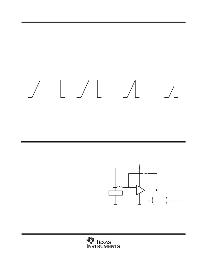
generally measured by monitoring the distortion level of the output while increasing the frequency of a sinusoidal
input signal until the maximum frequency is found above which the output contains significant distortion. The
full-peak response is defined as the maximum output frequency, without regard to distortion, above which full
peak-to-peak output swing cannot be maintained.
Because there is no industry-wide accepted value for significant distortion, the full-peak response is specified
in this data sheet and is measured using the circuit of Figure 35. The initial setup involves the use of a sinusoidal
input to determine the maximum peak-to-peak output of the device (the amplitude of the sinusoidal wave is
increased until clipping occurs). The sinusoidal wave is then replaced with a square wave of the same
amplitude. The frequency is then increased until the maximum peak-to-peak output can no longer be maintained
(Figure 39). A square wave is used to allow a more accurate determination of the point at which the maximum
peak-to-peak output is reached.
(d) f > BOM
(c) f = BOM
(b) BOM > f > 100 Hz
(a) f = 100 Hz
Figure 39. Full-Power-Response Output Signal
test time
Inadequate test time is a frequent problem, especially when testing CMOS devices in a high-volume,
short-test-time environment. Internal capacitances are inherently higher in CMOS than in bipolar and BiFET
devices, and require longer test times than their bipolar and BiFET counterparts. The problem becomes more
pronounced with reduced supply levels and lower temperatures.
APPLICATION INFORMATION
single-supply operation
While the TLV234x performs well using dual-
power supplies (also called balanced or split
supplies), the design is optimized for single-
supply operation. This includes an input common-
mode voltage range that encompasses ground as
well as an output voltage range that pulls down to
ground. The supply voltage range extends down
to 2 V, thus allowing operation with supply levels
commonly available for TTL and HCMOS.
Many single-supply applications require that a
voltage be applied to one input to establish a
reference level that is above ground. This virtual
ground can be generated using two large
resistors, but a preferred technique is to use a
virtual-ground generator such as the TLE2426
(see Figure 40).
–
+
TLE2426
VO
VI
R1
R2
VDD
Figure 40. Inverting Amplifier With
Voltage Reference
VO
VDD– VI
2
R2
R1
VDD
2
相关PDF资料 |
PDF描述 |
|---|---|
| TLV2344ID | LinCMOSE LOW-VOLTAGE HIGH-SPEED OPERATIONAL AMPLIFIERS |
| TLV2344Y | LinCMOSE LOW-VOLTAGE HIGH-SPEED OPERATIONAL AMPLIFIERS |
| TLV2361(中文) | Single High-Performance, Low-Voltage OP AMP(高性能,可编程低电压单运放) |
| TLV2362(中文) | Dual High-Performance, Low-Voltage OP AMP(高性能,可编程低电压双运放) |
| TLV2432(中文) | Advanced Lincmos Rail-TO-Rail Output Wide-Input-Voltage Dual OP AMP(宽输入电压,低功耗,中速,高输出驱动双运放) |
相关代理商/技术参数 |
参数描述 |
|---|---|
| TLV2344 | 制造商:TI 制造商全称:Texas Instruments 功能描述:LinCMOSE LOW-VOLTAGE HIGH-SPEED OPERATIONAL AMPLIFIERS |
| TLV2344ID | 功能描述:运算放大器 - 运放 Quad LiNCMOS RoHS:否 制造商:STMicroelectronics 通道数量:4 共模抑制比(最小值):63 dB 输入补偿电压:1 mV 输入偏流(最大值):10 pA 工作电源电压:2.7 V to 5.5 V 安装风格:SMD/SMT 封装 / 箱体:QFN-16 转换速度:0.89 V/us 关闭:No 输出电流:55 mA 最大工作温度:+ 125 C 封装:Reel |
| TLV2344IDG4 | 功能描述:运算放大器 - 运放 Quad LiNCMOS RoHS:否 制造商:STMicroelectronics 通道数量:4 共模抑制比(最小值):63 dB 输入补偿电压:1 mV 输入偏流(最大值):10 pA 工作电源电压:2.7 V to 5.5 V 安装风格:SMD/SMT 封装 / 箱体:QFN-16 转换速度:0.89 V/us 关闭:No 输出电流:55 mA 最大工作温度:+ 125 C 封装:Reel |
| TLV2344IN | 功能描述:运算放大器 - 运放 Quad LiNCMOS RoHS:否 制造商:STMicroelectronics 通道数量:4 共模抑制比(最小值):63 dB 输入补偿电压:1 mV 输入偏流(最大值):10 pA 工作电源电压:2.7 V to 5.5 V 安装风格:SMD/SMT 封装 / 箱体:QFN-16 转换速度:0.89 V/us 关闭:No 输出电流:55 mA 最大工作温度:+ 125 C 封装:Reel |
| TLV2344INE4 | 功能描述:运算放大器 - 运放 Quad LinCMOS Lo-Vltg High-Speed RoHS:否 制造商:STMicroelectronics 通道数量:4 共模抑制比(最小值):63 dB 输入补偿电压:1 mV 输入偏流(最大值):10 pA 工作电源电压:2.7 V to 5.5 V 安装风格:SMD/SMT 封装 / 箱体:QFN-16 转换速度:0.89 V/us 关闭:No 输出电流:55 mA 最大工作温度:+ 125 C 封装:Reel |
发布紧急采购,3分钟左右您将得到回复。