- 您现在的位置:买卖IC网 > PDF目录10705 > TLV2354INE4 (Texas Instruments)IC DIFF COMPARATOR QUAD 14-DIP PDF资料下载
参数资料
| 型号: | TLV2354INE4 |
| 厂商: | Texas Instruments |
| 文件页数: | 3/19页 |
| 文件大小: | 0K |
| 描述: | IC DIFF COMPARATOR QUAD 14-DIP |
| 标准包装: | 25 |
| 系列: | LinCMOS™ |
| 类型: | 差分 |
| 元件数: | 4 |
| 输出类型: | CMOS,MOS,开路漏极,TTL |
| 电压 - 电源,单路/双路(±): | 2 V ~ 8 V |
| 电压 - 输入偏移(最小值): | 5mV @ 5V |
| 电流 - 输入偏压(最小值): | 5pA @ 5V |
| 电流 - 输出(标准): | 20mA |
| 电流 - 静态(最大值): | 800µA |
| 工作温度: | -40°C ~ 85°C |
| 封装/外壳: | 14-DIP(0.300",7.62mm) |
| 安装类型: | 通孔 |
| 包装: | 管件 |
TLV2354, TLV2354Y
LinCMOS
QUADRUPLE LOW-VOLTAGE DIFFERENTIAL COMPARATORS
SLCS012C – MAY 1992 – REVISED AUGUST 2000
11
POST OFFICE BOX 655303
DALLAS, TEXAS 75265
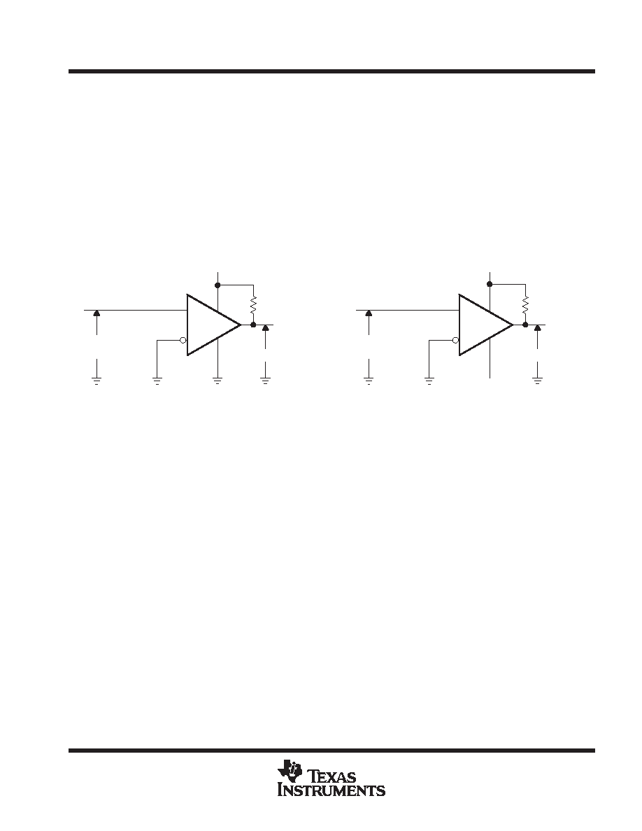
PARAMETER MEASUREMENT INFORMATION
The digital output stage of the TLV2354 can be damaged if it is held in the linear region of the transfer curve.
Conventional operational amplifier/comparator testing incorporates the use of a servo loop that is designed to force
the device output to a level within this linear region. Since the servo-loop method of testing cannot be used, the
following alternatives for measuring parameters such as input offset voltage, common-mode rejection, etc., are
offered.
To verify that the input offset voltage falls within the limits specified, the limit value is applied to the input as shown
in Figure 9(a). With the noninverting input positive with respect to the inverting input, the output should be high. With
the input polarity reversed, the output should be low.
A similar test can be made to verify the input offset voltage at the common-mode extremes. The supply voltages can
be slewed as shown in Figure 9(b) for the VICR test rather than changing the input voltages to provide greater
accuracy.
+
–
5 V
Applied VIO
Limit
VO
+
–
1 V
Applied VIO
Limit
VO
– 4 V
(a) VIO WITH VIC = 0
(b) VIO WITH VIC = 4 V
5.1 k
5.1 k
Figure 9. Method for Verifying That Input Offset Voltage Is Within Specified Limits
A close approximation of the input offset voltage can be obtained by using a binary search method to vary the
differential input voltage while monitoring the output state. When the applied input voltage differential is equal but
opposite in polarity to the input offset voltage, the output changes states.
相关PDF资料 |
PDF描述 |
|---|---|
| VI-J1J-MY-F2 | CONVERTER MOD DC/DC 36V 50W |
| VI-J1J-MY-F1 | CONVERTER MOD DC/DC 36V 50W |
| VI-272-IX-B1 | CONVERTER MOD DC/DC 15V 75W |
| VI-J1L-MY-F2 | CONVERTER MOD DC/DC 28V 50W |
| VE-B5K-MY-B1 | CONVERTER MOD DC/DC 40V 50W |
相关代理商/技术参数 |
参数描述 |
|---|---|
| TLV2354IPW | 功能描述:校验器 IC Quad Lo-Vltg LinCMOS Differential RoHS:否 制造商:STMicroelectronics 产品: 比较器类型: 通道数量: 输出类型:Push-Pull 电源电压-最大:5.5 V 电源电压-最小:1.1 V 补偿电压(最大值):6 mV 电源电流(最大值):1350 nA 响应时间: 最大工作温度:+ 125 C 安装风格:SMD/SMT 封装 / 箱体:SC-70-5 封装:Reel |
| TLV2354IPWG4 | 功能描述:校验器 IC Quad Lo-Vltg LinCMOS Differential RoHS:否 制造商:STMicroelectronics 产品: 比较器类型: 通道数量: 输出类型:Push-Pull 电源电压-最大:5.5 V 电源电压-最小:1.1 V 补偿电压(最大值):6 mV 电源电流(最大值):1350 nA 响应时间: 最大工作温度:+ 125 C 安装风格:SMD/SMT 封装 / 箱体:SC-70-5 封装:Reel |
| TLV2354IPWLE | 制造商:TI 制造商全称:Texas Instruments 功能描述:LinCMOSE QUADRUPLE LOW-VOLTAGE DIFFERENTIAL COMPARATORS |
| TLV2354IPWR | 功能描述:校验器 IC Quad Diff RoHS:否 制造商:STMicroelectronics 产品: 比较器类型: 通道数量: 输出类型:Push-Pull 电源电压-最大:5.5 V 电源电压-最小:1.1 V 补偿电压(最大值):6 mV 电源电流(最大值):1350 nA 响应时间: 最大工作温度:+ 125 C 安装风格:SMD/SMT 封装 / 箱体:SC-70-5 封装:Reel |
| TLV2354IPWRG4 | 功能描述:校验器 IC Quad Lo-Vltg LinCMOS Differential RoHS:否 制造商:STMicroelectronics 产品: 比较器类型: 通道数量: 输出类型:Push-Pull 电源电压-最大:5.5 V 电源电压-最小:1.1 V 补偿电压(最大值):6 mV 电源电流(最大值):1350 nA 响应时间: 最大工作温度:+ 125 C 安装风格:SMD/SMT 封装 / 箱体:SC-70-5 封装:Reel |
发布紧急采购,3分钟左右您将得到回复。