- 您现在的位置:买卖IC网 > PDF目录10705 > TLV2354INE4 (Texas Instruments)IC DIFF COMPARATOR QUAD 14-DIP PDF资料下载
参数资料
| 型号: | TLV2354INE4 |
| 厂商: | Texas Instruments |
| 文件页数: | 4/19页 |
| 文件大小: | 0K |
| 描述: | IC DIFF COMPARATOR QUAD 14-DIP |
| 标准包装: | 25 |
| 系列: | LinCMOS™ |
| 类型: | 差分 |
| 元件数: | 4 |
| 输出类型: | CMOS,MOS,开路漏极,TTL |
| 电压 - 电源,单路/双路(±): | 2 V ~ 8 V |
| 电压 - 输入偏移(最小值): | 5mV @ 5V |
| 电流 - 输入偏压(最小值): | 5pA @ 5V |
| 电流 - 输出(标准): | 20mA |
| 电流 - 静态(最大值): | 800µA |
| 工作温度: | -40°C ~ 85°C |
| 封装/外壳: | 14-DIP(0.300",7.62mm) |
| 安装类型: | 通孔 |
| 包装: | 管件 |
TLV2354, TLV2354Y
LinCMOS
QUADRUPLE LOW-VOLTAGE DIFFERENTIAL COMPARATORS
SLCS012C – MAY 1992 – REVISED AUGUST 2000
12
POST OFFICE BOX 655303
DALLAS, TEXAS 75265
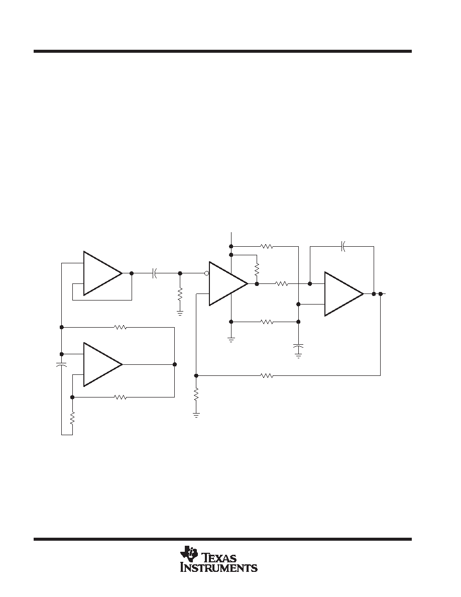
PARAMETER MEASUREMENT INFORMATION
Figure 10 illustrates a practical circuit for direct dc measurement of input offset voltage that does not bias the
comparator in the linear region. The circuit consists of a switching-mode servo loop in which U1a generates a
triangular waveform of approximately 20-mV amplitude. U1b acts as a buffer, with C2 and R4 removing any residual
dc offset. The signal is then applied to the inverting input of the comparator under test while the noninverting input
is driven by the output of the integrator formed by U1c through the voltage divider formed by R9 and R10. The loop
reaches a stable operating point when the output of the comparator under test has a duty cycle of exactly 50%, which
can only occur when the incoming triangle wave is sliced symmetrically or when the voltage at the noninverting input
exactly equals the input offset voltage.
Voltage dividers R9 and R10 provide a step up of the input offset voltage by a factor of 100 to make measurement
easier. The values of R5, R8, R9, and R10 can significantly influence the accuracy of the reading; therefore, it is
suggested that their tolerance level be 1% or lower.
Measuring the extremely low values of input current requires isolation from all other sources of leakage current and
compensation for the leakage of the test socket and board. With a good picoammeter, the socket and board leakage
can be measured with no device in the socket. Subsequently, this open-socket leakage value can be subtracted from
the measurement obtained with a device in the socket to obtain the actual input current of the device.
–
+
DUT
VDD
+
–
+
–
+
C2
1
F
R4
47 k
R5
1.8 k
, 1%
C3
0.68
F
U1c 1/4
TLV2354
U1b 1/4
TLV2354
U1a 1/4
TLV2354
R7
1 M
R8
1.8 k
, 1%
R9
10 k
, 1%
R1
240 k
R2
10 k
C1
0.1
F
R3
100
C4
0.1
F
Integrator
R10
100
, 1%
Buffer
Triangle
Generator
VIO
(
×100)
R6
5.1 k
Figure 10. Circuit for Input Offset Voltage Measurement
相关PDF资料 |
PDF描述 |
|---|---|
| VI-J1J-MY-F2 | CONVERTER MOD DC/DC 36V 50W |
| VI-J1J-MY-F1 | CONVERTER MOD DC/DC 36V 50W |
| VI-272-IX-B1 | CONVERTER MOD DC/DC 15V 75W |
| VI-J1L-MY-F2 | CONVERTER MOD DC/DC 28V 50W |
| VE-B5K-MY-B1 | CONVERTER MOD DC/DC 40V 50W |
相关代理商/技术参数 |
参数描述 |
|---|---|
| TLV2354IPW | 功能描述:校验器 IC Quad Lo-Vltg LinCMOS Differential RoHS:否 制造商:STMicroelectronics 产品: 比较器类型: 通道数量: 输出类型:Push-Pull 电源电压-最大:5.5 V 电源电压-最小:1.1 V 补偿电压(最大值):6 mV 电源电流(最大值):1350 nA 响应时间: 最大工作温度:+ 125 C 安装风格:SMD/SMT 封装 / 箱体:SC-70-5 封装:Reel |
| TLV2354IPWG4 | 功能描述:校验器 IC Quad Lo-Vltg LinCMOS Differential RoHS:否 制造商:STMicroelectronics 产品: 比较器类型: 通道数量: 输出类型:Push-Pull 电源电压-最大:5.5 V 电源电压-最小:1.1 V 补偿电压(最大值):6 mV 电源电流(最大值):1350 nA 响应时间: 最大工作温度:+ 125 C 安装风格:SMD/SMT 封装 / 箱体:SC-70-5 封装:Reel |
| TLV2354IPWLE | 制造商:TI 制造商全称:Texas Instruments 功能描述:LinCMOSE QUADRUPLE LOW-VOLTAGE DIFFERENTIAL COMPARATORS |
| TLV2354IPWR | 功能描述:校验器 IC Quad Diff RoHS:否 制造商:STMicroelectronics 产品: 比较器类型: 通道数量: 输出类型:Push-Pull 电源电压-最大:5.5 V 电源电压-最小:1.1 V 补偿电压(最大值):6 mV 电源电流(最大值):1350 nA 响应时间: 最大工作温度:+ 125 C 安装风格:SMD/SMT 封装 / 箱体:SC-70-5 封装:Reel |
| TLV2354IPWRG4 | 功能描述:校验器 IC Quad Lo-Vltg LinCMOS Differential RoHS:否 制造商:STMicroelectronics 产品: 比较器类型: 通道数量: 输出类型:Push-Pull 电源电压-最大:5.5 V 电源电压-最小:1.1 V 补偿电压(最大值):6 mV 电源电流(最大值):1350 nA 响应时间: 最大工作温度:+ 125 C 安装风格:SMD/SMT 封装 / 箱体:SC-70-5 封装:Reel |
发布紧急采购,3分钟左右您将得到回复。