- 您现在的位置:买卖IC网 > PDF目录98252 > TLV2553IDWRQ1 (TEXAS INSTRUMENTS INC) 11-CH 12-BIT SUCCESSIVE APPROXIMATION ADC, SERIAL ACCESS, PDSO20 PDF资料下载
参数资料
| 型号: | TLV2553IDWRQ1 |
| 厂商: | TEXAS INSTRUMENTS INC |
| 元件分类: | ADC |
| 英文描述: | 11-CH 12-BIT SUCCESSIVE APPROXIMATION ADC, SERIAL ACCESS, PDSO20 |
| 封装: | GREEN, PLASTIC, SOIC-20 |
| 文件页数: | 14/28页 |
| 文件大小: | 414K |
| 代理商: | TLV2553IDWRQ1 |
第1页第2页第3页第4页第5页第6页第7页第8页第9页第10页第11页第12页第13页当前第14页第15页第16页第17页第18页第19页第20页第21页第22页第23页第24页第25页第26页第27页第28页
Power Up and Initialization
Data Input
www.ti.com ..................................................................................................................................................................................................... SLAS579 – APRIL 2009
After power up, CS must be taken from high to low to begin an I/O cycle. The EOC pin is initially high, and the
configuration register is set to all zeroes. The contents of the output data register are random, and the first
conversion result should be ignored. To initialize during operation, CS is taken high and is then returned low to
begin the next I/O cycle. The first conversion after the device has returned from the power-down state may not
read accurately due to internal device settling.
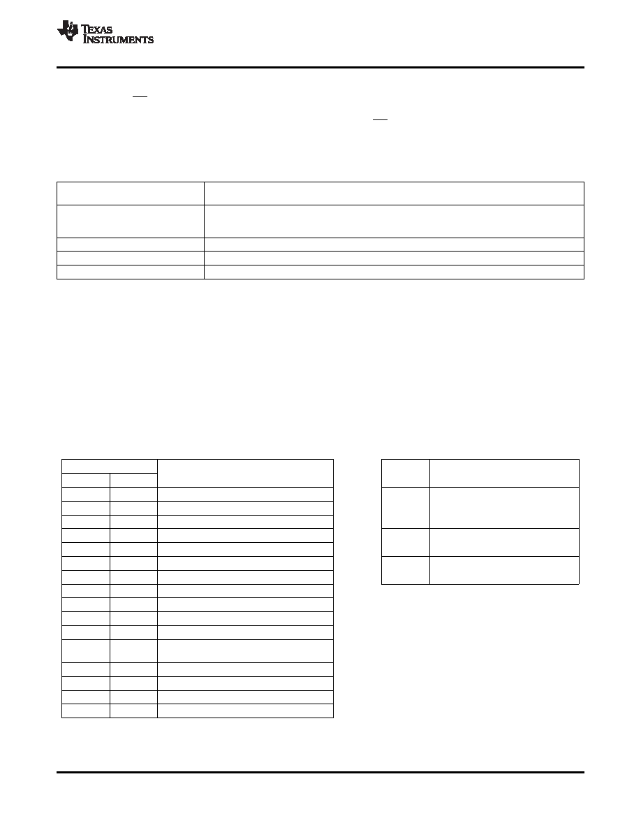
Table 1. Operational Terminology
The entire I/O CLOCK sequence that transfers address and control data into the data register and
Current (N) I/O cycle
clocks the digital result from the previous conversion from DATA OUT
The conversion cycle starts immediately after the current I/O cycle. The end of the current I/O cycle
Current (N) conversion cycle
is the last clock falling edge in the I/O CLOCK sequence. The current conversion result is loaded
into the output register when conversion is complete.
Current (N) conversion result
The current conversion result is serially shifted out on the next I/O cycle.
Previous (N – 1) conversion cycle
The conversion cycle just prior to the current I/O cycle
Next (N + 1) I/O cycle
The I/O period that follows the current conversion cycle
Example
In 12-bit mode, the result of the current conversion cycle is a 12-bit serial-data stream clocked out during the
next I/O cycle. The current I/O cycle must be exactly 12 bits long to maintain synchronization, even when this
corrupts the output data from the previous conversion. The current conversion is begun immediately after the
twelfth falling edge of the current I/O cycle.
The data input is internally connected to an 8-bit serial-input address and control register. The register defines
the operation of the converter and the output data length. The host provides the input data byte with the MSB
first. Each data bit is clocked in on the rising edge of the I/O CLOCK sequence (see Table 2 for the data
input-register format).
Table 2. Command Set (CMR) and Configuration
SDI D[7:4]
CFGR1
COMMAND
CONFIGURATION
BINARY
HEX
SDI D[3:0]
0000
0
SELECT analog input channel 0
01: 8-bit output length
0001
1
SELECT analog input channel 1
D[3:2]
X0: 12-bit output length(1)
0010
2
SELECT analog input channel 2
11: 16-bit output length
0011
3
SELECT analog input channel 3
0: MSB out first
D1
0100
4
SELECT analog input channel 4
1: LSB out first
0101
5
SELECT analog input channel 5
0: Unipolar binary
D0
0110
6
SELECT analog input channel 6
1: Bipolar 2s complement
0111
7
SELECT analog input channel 7
1000
8
SELECT analog input channel 8
1001
9
SELECT analog input channel 9
1010
A
SELECT analog input channel 10
SELECT TEST,
1011
B
Voltage = (VREF+ + VREF–)/2
1100
C
SELECT TEST, Voltage = REFM
1101
D
SELECT TEST, Voltage = REFP
1110
E
SW POWERDOWN (analog + reference)
1111
F
Reserved
(1)
Select 12-bit output mode to achieve 200-KSPS sampling rate.
Copyright 2009, Texas Instruments Incorporated
21
Product Folder Link(s): TLV2553-Q1
相关PDF资料 |
PDF描述 |
|---|---|
| TLV2556IDWRG4 | 11-CH 12-BIT SUCCESSIVE APPROXIMATION ADC, SERIAL ACCESS, PDSO20 |
| TLV2556IPW | 11-CH 12-BIT SUCCESSIVE APPROXIMATION ADC, SERIAL ACCESS, PDSO20 |
| TLV2556IDWR | 11-CH 12-BIT SUCCESSIVE APPROXIMATION ADC, SERIAL ACCESS, PDSO20 |
| TLV2556IPWR | 11-CH 12-BIT SUCCESSIVE APPROXIMATION ADC, SERIAL ACCESS, PDSO20 |
| TLV2556IDW | 11-CH 12-BIT SUCCESSIVE APPROXIMATION ADC, SERIAL ACCESS, PDSO20 |
相关代理商/技术参数 |
参数描述 |
|---|---|
| TLV2553IPW | 功能描述:模数转换器 - ADC 12-Bit 200 KSPS 11 Ch Lo-Pwr RoHS:否 制造商:Texas Instruments 通道数量:2 结构:Sigma-Delta 转换速率:125 SPs to 8 KSPs 分辨率:24 bit 输入类型:Differential 信噪比:107 dB 接口类型:SPI 工作电源电压:1.7 V to 3.6 V, 2.7 V to 5.25 V 最大工作温度:+ 85 C 安装风格:SMD/SMT 封装 / 箱体:VQFN-32 |
| TLV2553IPWG4 | 功能描述:模数转换器 - ADC 12-Bit 200 KSPS 11 Ch Lo-Pwr RoHS:否 制造商:Texas Instruments 通道数量:2 结构:Sigma-Delta 转换速率:125 SPs to 8 KSPs 分辨率:24 bit 输入类型:Differential 信噪比:107 dB 接口类型:SPI 工作电源电压:1.7 V to 3.6 V, 2.7 V to 5.25 V 最大工作温度:+ 85 C 安装风格:SMD/SMT 封装 / 箱体:VQFN-32 |
| TLV2553IPWR | 功能描述:模数转换器 - ADC 12-Bit 200 KSPS 11 Ch Lo-Pwr RoHS:否 制造商:Texas Instruments 通道数量:2 结构:Sigma-Delta 转换速率:125 SPs to 8 KSPs 分辨率:24 bit 输入类型:Differential 信噪比:107 dB 接口类型:SPI 工作电源电压:1.7 V to 3.6 V, 2.7 V to 5.25 V 最大工作温度:+ 85 C 安装风格:SMD/SMT 封装 / 箱体:VQFN-32 |
| TLV2553IPWRG4 | 功能描述:模数转换器 - ADC 12-Bit 200 KSPS 11 Ch Lo-Pwr RoHS:否 制造商:Texas Instruments 通道数量:2 结构:Sigma-Delta 转换速率:125 SPs to 8 KSPs 分辨率:24 bit 输入类型:Differential 信噪比:107 dB 接口类型:SPI 工作电源电压:1.7 V to 3.6 V, 2.7 V to 5.25 V 最大工作温度:+ 85 C 安装风格:SMD/SMT 封装 / 箱体:VQFN-32 |
| TLV2553IPWRQ1 | 功能描述:12 Bit Analog to Digital Converter 11 Input 1 SAR 20-TSSOP 制造商:texas instruments 系列:- 包装:剪切带(CT) 零件状态:有效 位数:12 采样率(每秒):200k 输入数:11 输入类型:单端 数据接口:SPI 配置:MUX-S/H-ADC 无线电 - S/H:ADC:1:1 A/D 转换器数:1 架构:SAR 参考类型:外部 电压 - 电源,模拟:2.7 V ~ 5.5 V 电压 - 电源,数字:2.7 V ~ 5.5 V 特性:- 工作温度:-40°C ~ 85°C 封装/外壳:20-TSSOP(0.173",4.40mm 宽) 供应商器件封装:20-TSSOP 标准包装:1 |
发布紧急采购,3分钟左右您将得到回复。