- 您现在的位置:买卖IC网 > PDF目录98252 > TLV320AIC14I (TEXAS INSTRUMENTS INC) SPECIALTY CONSUMER CIRCUIT, PDSO30 PDF资料下载
参数资料
| 型号: | TLV320AIC14I |
| 厂商: | TEXAS INSTRUMENTS INC |
| 元件分类: | 消费家电 |
| 英文描述: | SPECIALTY CONSUMER CIRCUIT, PDSO30 |
| 封装: | PLASTIC, TSSOP-30 |
| 文件页数: | 4/54页 |
| 文件大小: | 450K |
| 代理商: | TLV320AIC14I |
第1页第2页第3页当前第4页第5页第6页第7页第8页第9页第10页第11页第12页第13页第14页第15页第16页第17页第18页第19页第20页第21页第22页第23页第24页第25页第26页第27页第28页第29页第30页第31页第32页第33页第34页第35页第36页第37页第38页第39页第40页第41页第42页第43页第44页第45页第46页第47页第48页第49页第50页第51页第52页第53页第54页
2–1
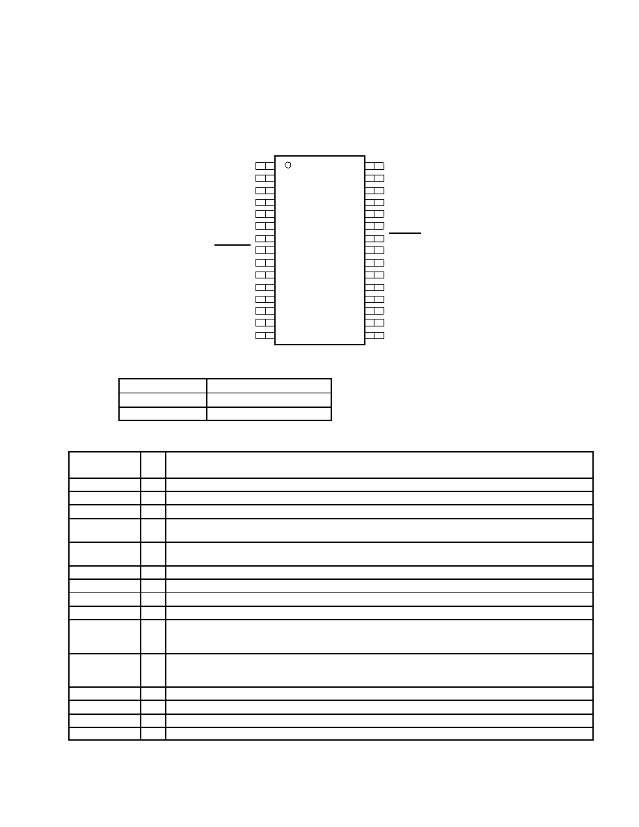
2 Terminal Descriptions
1
2
3
4
5
6
7
8
9
10
11
12
13
14
15
30
29
28
27
26
25
24
23
22
21
20
19
18
17
16
IOVSS
IOVDD
FSD
FS
DOUT
DIN
M/S
PWRDN
OUTM1
OUTP1
DRVDD
DRVSS
NC
DVSS
DVDD
SCLK
SDA
SCL
MCLK
RESET
INP1
INM1
BIAS
INM2
INP2
MICIN
AVDD
AVSS
DBT PACKAGE
(TOP VIEW)
2.1
Ordering Information
TA
30-TSSOP DBT PACKAGE
0
°C to 70°C
TLV320AIC14C
–40
°C to 85°C
TLV320AIC14I
2.2
Terminal Functions
TERMINAL
I/O
DESCRIPTION
NAME
NO.
I/O
DESCRIPTION
AVDD
17
I
Analog power supply
AVSS
16
I
Analog ground
BIAS
21
O
Bias output voltage is software selectable between 1.35 V and 2.35 V. Its output current is 5 mA.
DIN
6
I
Data input. DIN receives the DAC input data and register data from the external DSP (digital signal processor) and is
synchronized to SCLK and FS. Data is latched at the falling edge of SCLK when FS is low.
DOUT
5
O
Data output. DOUT transmits the ADC output bits and registers data, and is synchronized to SCLK and FS. Data is
sent out at the rising edge of SCLK when FS is low. Outside data/control frame, DOUT is put in 3-state.
DRVDD
11
I
Analog power supply for the 600-
driver
DRVSS
12
I
Analog ground for the 600-
driver
DVDD
29
I
Digital power supply
DVSS
30
I
Digital ground
FS
4
I/O
Frame sync. When FS goes low, DIN begins receiving data bits and DOUT begins transmitting data bits. In master
mode, FS is internally generated and is low during the data transmission to DIN and from DOUT. In slave mode, FS is
externally generated.
FSD
3
O
Frame sync delayed output. The FSD output synchronizes a slave device to the frame sync of the master device. FSD
is applied to the slave FS input and is the same duration as the master FS signal. This pin must be pulled low if AIC14 is
a stand-alone slave. It may be pulled high if the AIC14 is a stand-alone master or the last slave in the cascade.
INM1
22
I
Inverting analog input 1. It must be connected to AVSS if not used.
INM2
20
I
Inverting analog input 2. It must be connected to AVSS if not used.
INP1
23
I
Noninverting analog input 1. It must be connected to AVSS if not used.
INP2
19
I
Noninverting analog input 2. It must be connected to AVSS if not used.
相关PDF资料 |
PDF描述 |
|---|---|
| TLV320AIC22PT | SPECIALTY CONSUMER CIRCUIT, PQFP48 |
| TLV320AIC22PTR | SPECIALTY CONSUMER CIRCUIT, PQFP48 |
| TLV320AIC23BGQE | SPECIALTY CONSUMER CIRCUIT, PBGA80 |
| TLV320AIC23BIGQE | SPECIALTY CONSUMER CIRCUIT, PBGA80 |
| TLV320AIC23BIPW | SPECIALTY CONSUMER CIRCUIT, PDSO28 |
相关代理商/技术参数 |
参数描述 |
|---|---|
| TLV320AIC14IDBT | 功能描述:接口—CODEC Lo-Pwr Mono Voice Band CODEC RoHS:否 制造商:Texas Instruments 类型: 分辨率: 转换速率:48 kSPs 接口类型:I2C ADC 数量:2 DAC 数量:4 工作电源电压:1.8 V, 2.1 V, 2.3 V to 5.5 V 最大工作温度:+ 85 C 安装风格:SMD/SMT 封装 / 箱体:DSBGA-81 封装:Reel |
| TLV320AIC14IDBT-1 | 制造商:Rochester Electronics LLC 功能描述: 制造商:Texas Instruments 功能描述: |
| TLV320AIC14IDBTG4 | 功能描述:接口—CODEC Lo-Pwr Mono Voice Band CODEC RoHS:否 制造商:Texas Instruments 类型: 分辨率: 转换速率:48 kSPs 接口类型:I2C ADC 数量:2 DAC 数量:4 工作电源电压:1.8 V, 2.1 V, 2.3 V to 5.5 V 最大工作温度:+ 85 C 安装风格:SMD/SMT 封装 / 箱体:DSBGA-81 封装:Reel |
| TLV320AIC14IDBTR | 功能描述:接口—CODEC Lo-Pwr Mono Voice Band CODEC RoHS:否 制造商:Texas Instruments 类型: 分辨率: 转换速率:48 kSPs 接口类型:I2C ADC 数量:2 DAC 数量:4 工作电源电压:1.8 V, 2.1 V, 2.3 V to 5.5 V 最大工作温度:+ 85 C 安装风格:SMD/SMT 封装 / 箱体:DSBGA-81 封装:Reel |
| TLV320AIC14IDBTRG4 | 功能描述:接口—CODEC Lo-Pwr Mono Voice Band CODEC RoHS:否 制造商:Texas Instruments 类型: 分辨率: 转换速率:48 kSPs 接口类型:I2C ADC 数量:2 DAC 数量:4 工作电源电压:1.8 V, 2.1 V, 2.3 V to 5.5 V 最大工作温度:+ 85 C 安装风格:SMD/SMT 封装 / 箱体:DSBGA-81 封装:Reel |
发布紧急采购,3分钟左右您将得到回复。