- 您现在的位置:买卖IC网 > PDF目录98253 > TLV320AIC24KIPFBRG4 (TEXAS INSTRUMENTS INC) SPECIALTY CONSUMER CIRCUIT, PQFP48 PDF资料下载
参数资料
| 型号: | TLV320AIC24KIPFBRG4 |
| 厂商: | TEXAS INSTRUMENTS INC |
| 元件分类: | 消费家电 |
| 英文描述: | SPECIALTY CONSUMER CIRCUIT, PQFP48 |
| 封装: | GREEN, PLASTIC, TQFP-48 |
| 文件页数: | 14/52页 |
| 文件大小: | 981K |
| 代理商: | TLV320AIC24KIPFBRG4 |
第1页第2页第3页第4页第5页第6页第7页第8页第9页第10页第11页第12页第13页当前第14页第15页第16页第17页第18页第19页第20页第21页第22页第23页第24页第25页第26页第27页第28页第29页第30页第31页第32页第33页第34页第35页第36页第37页第38页第39页第40页第41页第42页第43页第44页第45页第46页第47页第48页第49页第50页第51页第52页
www.ti.com
Functional Description
Operating Frequencies
MCLK
1/P
1/(MN)
128FS
(devnum x mode)/(MNP)
SCLK
1/(16 x mode x devnum)
FS
en_dll
Digital
X 8
(DLL)
SCLK may not be a uniform clock depending upon value of devnum, mode, and MNP.
.
M = 1 - 128
N = 1 - 16
P = 1 - 8
When:
P1 = 8, DLL(PLL) is Enabled
devnum = Number of Channels in Cascade.
Note That for a Standalone Device, devnum = 2.
Mode = 1 (For Continious Data Transfer Mode)
Mode = 2 (For Programming Mode)
TLV320AIC20, TLV320AIC21
TLV320AIC24, TLV320AIC25
TLV320AIC20K, TLV320AIC24K
SLAS363D – MARCH 2002 – REVISED APRIL 2005
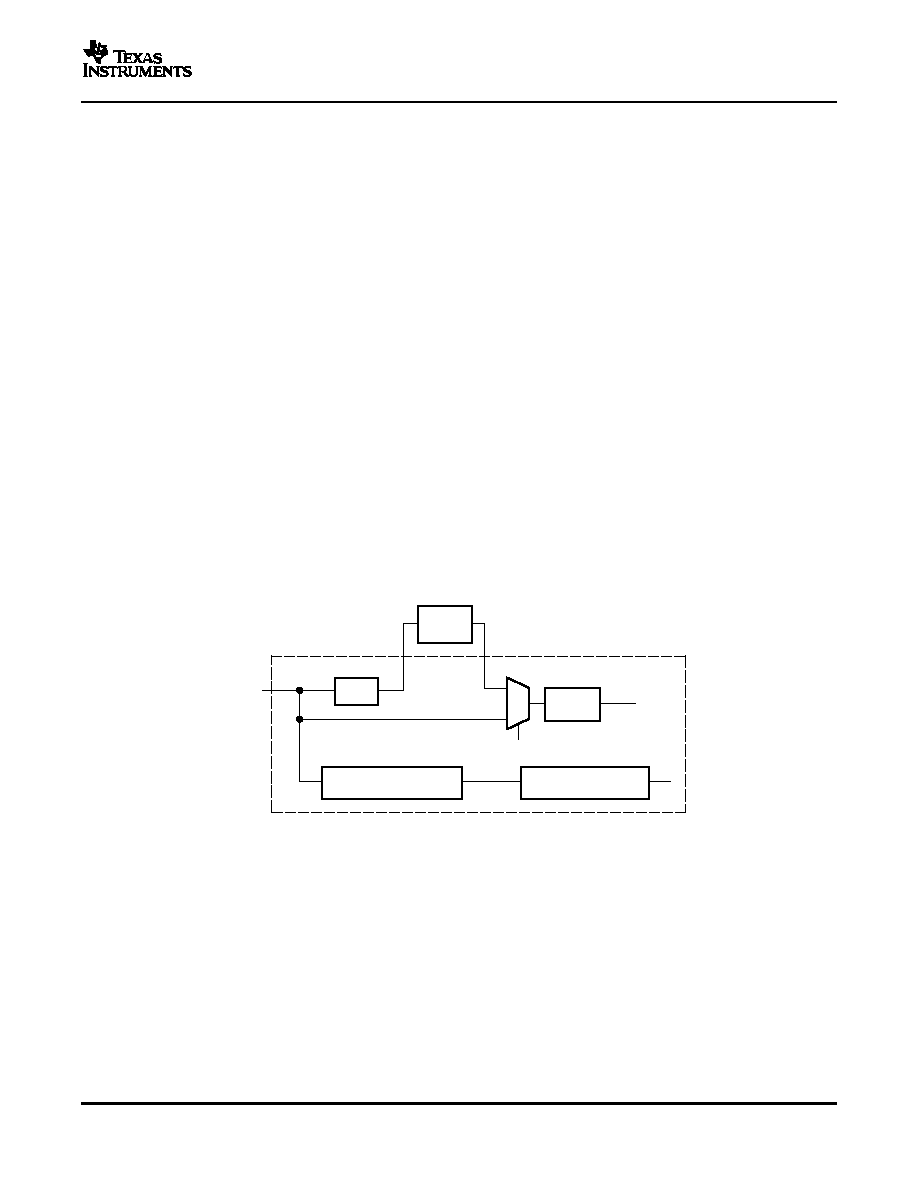
The sampling frequency is the frequency of the frame sync (FS) signal where falling edge starts digital-data
transfer for both ADC and DAC. The sampling frequency is derived from the master clock (MCLK) input by the
following equations:
Coarse sampling frequency (default):
– The coarse sampling is selected by programming P = 8 in the control register 4, which is the default
configuration of AIC2x on power-up or reset.
– FS = Sampling (conversion) frequency = MCLK / (16 x M x N x 8)
Fine sampling frequency (see Note 5):
– FS = Sampling (conversion) frequency = MCLK/ (16 x M x N x P)
NOTE:
1. Use control register 4 to set the following values of M, N, and P
2. M = 1, 2, . . . , 128
3. N = 1, 2, . . . , 16
4. P = 1, 2, . . . , 8
5. The fine sampling rate needs an on-chip phase lock loop (frequency multiplier) to
generate internal clocks. The output of the PLL is only used to generate internal
clocks that are needed by the data converters. Other clocks such as the serial
interface clocks in master mode are not generated from the PLL output. The clock
generation scheme is as shown in Figure 18. The PLL requires the relationship
between MCLK and P to meet the following condition: 10 MHz
≤ (MCLK/P) ≤ 25
MHz.
Figure 18. Clock Timing
6. Selecting the Fine sampling mode turns on the analog PLL, which starts
generating after a finite time delay. The internal clocks are required to be present
in order to enable the DAC output drivers. Therefore, turning on any output drivers
immediately after turning on the PLL causes the output of the DAC to go to the
common-mode voltage. While using the PLL, the output drivers must first be
enabled before the PLL is enabled in order to ensure correct operation of the part.
This implies that register 6B for channel 1 and channel 2 in the codec must be
programmed before register 4.
21
相关PDF资料 |
PDF描述 |
|---|---|
| TLV320AIC20KIPFBRG4 | SPECIALTY CONSUMER CIRCUIT, PQFP48 |
| TLV320AIC26IRHBR | SPECIALTY CONSUMER CIRCUIT, PQCC32 |
| TLV320AIC26IRHB | SPECIALTY CONSUMER CIRCUIT, PQCC32 |
| TLV320AIC26IRHBG4 | SPECIALTY CONSUMER CIRCUIT, PQCC32 |
| TLV320AIC26IRHBRG4 | SPECIALTY CONSUMER CIRCUIT, PQCC32 |
相关代理商/技术参数 |
参数描述 |
|---|---|
| TLV320AIC25 | 制造商:TI 制造商全称:Texas Instruments 功能描述:PRODUCT NOTIFICATION |
| TLV320AIC25C | 制造商:TI 制造商全称:Texas Instruments 功能描述:Layout and Grounding Guidelines for TLV320AIC2x |
| TLV320AIC25CPFB | 功能描述:接口—CODEC Low Power Low IOVdd Dual Channel RoHS:否 制造商:Texas Instruments 类型: 分辨率: 转换速率:48 kSPs 接口类型:I2C ADC 数量:2 DAC 数量:4 工作电源电压:1.8 V, 2.1 V, 2.3 V to 5.5 V 最大工作温度:+ 85 C 安装风格:SMD/SMT 封装 / 箱体:DSBGA-81 封装:Reel |
| TLV320AIC25CPFBG4 | 功能描述:接口—CODEC 512 x 18 3.3-V Synch FIFO Memory RoHS:否 制造商:Texas Instruments 类型: 分辨率: 转换速率:48 kSPs 接口类型:I2C ADC 数量:2 DAC 数量:4 工作电源电压:1.8 V, 2.1 V, 2.3 V to 5.5 V 最大工作温度:+ 85 C 安装风格:SMD/SMT 封装 / 箱体:DSBGA-81 封装:Reel |
| TLV320AIC25CPFBR | 功能描述:接口—CODEC Low Power Low IOVdd Dual Channel RoHS:否 制造商:Texas Instruments 类型: 分辨率: 转换速率:48 kSPs 接口类型:I2C ADC 数量:2 DAC 数量:4 工作电源电压:1.8 V, 2.1 V, 2.3 V to 5.5 V 最大工作温度:+ 85 C 安装风格:SMD/SMT 封装 / 箱体:DSBGA-81 封装:Reel |
发布紧急采购,3分钟左右您将得到回复。