- 您现在的位置:买卖IC网 > PDF目录98253 > TLV320AIC24KIPFBRG4 (TEXAS INSTRUMENTS INC) SPECIALTY CONSUMER CIRCUIT, PQFP48 PDF资料下载
参数资料
| 型号: | TLV320AIC24KIPFBRG4 |
| 厂商: | TEXAS INSTRUMENTS INC |
| 元件分类: | 消费家电 |
| 英文描述: | SPECIALTY CONSUMER CIRCUIT, PQFP48 |
| 封装: | GREEN, PLASTIC, TQFP-48 |
| 文件页数: | 27/52页 |
| 文件大小: | 981K |
| 代理商: | TLV320AIC24KIPFBRG4 |
第1页第2页第3页第4页第5页第6页第7页第8页第9页第10页第11页第12页第13页第14页第15页第16页第17页第18页第19页第20页第21页第22页第23页第24页第25页第26页当前第27页第28页第29页第30页第31页第32页第33页第34页第35页第36页第37页第38页第39页第40页第41页第42页第43页第44页第45页第46页第47页第48页第49页第50页第51页第52页
www.ti.com
Control Register Programming
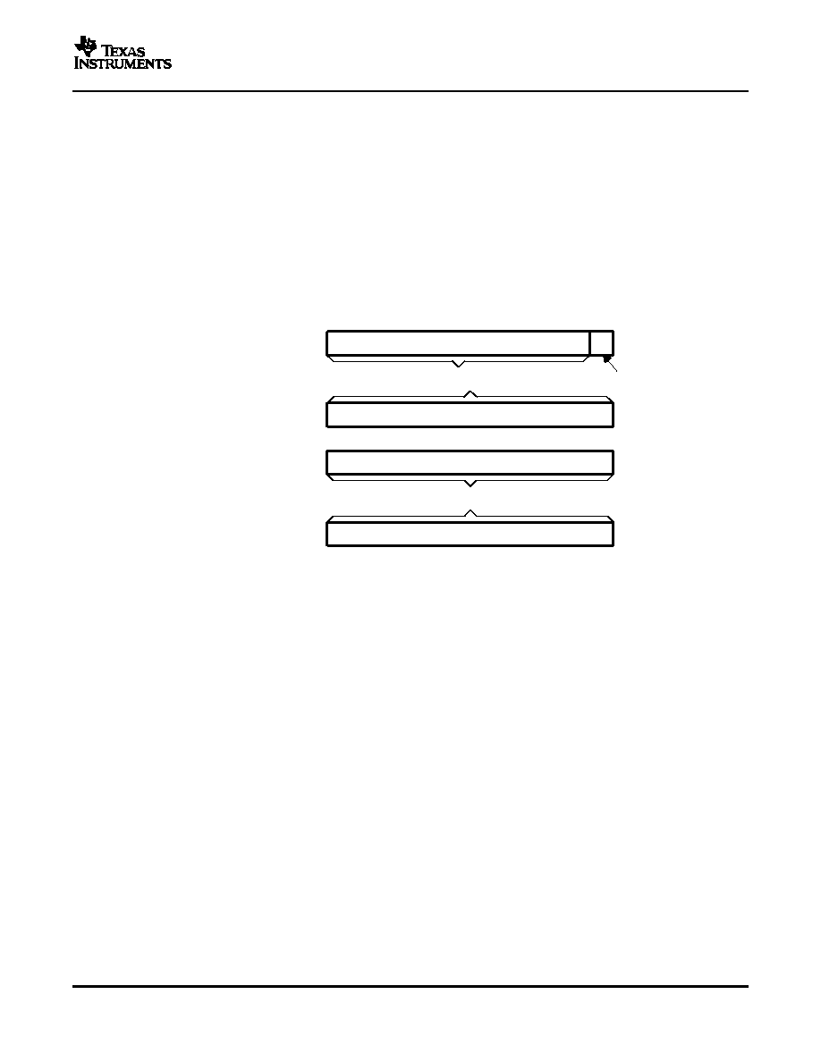
Data Frame Format
D0
D15 - D1
A/D and D/A Data
D15 - D0
A/D and D/A Data
D15 - D0
DIN
(15+1) Bit Mode
(Continuous Data Transfer Mode Only)
DOUT
(16 Bit A/D Data)
DIN
16 Bit Mode
DOUT
16 Bit Mode
Control Frame
Request
Control Frame Format (Programming Mode)
Broadcast Register Write
TLV320AIC20, TLV320AIC21
TLV320AIC24, TLV320AIC25
TLV320AIC20K, TLV320AIC24K
SLAS363D – MARCH 2002 – REVISED APRIL 2005
Each channel in the TLV320AIC2x contains six control registers that are used to program available modes of
operation. All register programming occurs during the control frame through DIN. New configuration takes effect
after a delay of one frame sync. The TLV320AIC2x is defaulted to the programming mode upon power up. Set bit
6 in control register 1 to switch to continuous data transfer mode. If the 15+1 data format of DIN has been
selected, the LSB of the DIN to 1 to switch from continuous data transfer mode to programming set mode.
Otherwise, either the device needs to be reset or the host port writes 0 to bit D6 of each codec's control register
1 during the continuous data transfer mode to switch back to the programming mode. The control registers are
replicated for each channel in the AIC2x, and these need to be programmed separately for the individual
channels. Register bits that control resources that are common to both channels are shadowed (i.e., writing to
the appropriate register bit of one channel is automatically reflected in the register bits for the other channel).
See the control register tables for a more detailed description of the exact register bits that are shadowed.
Figure 28. Data Frame Format
During the control frame, the DSP sends 16-bit words to each codec's time slot SMARTDM(TM) through DIN to
read or write control registers in each codec shown in Table 4. The upper byte (Bits D15-D8) of the 16-bit
control-frame word defines the read/write command. Bits D15-D13 define the control register address with
register content occupied the lower byte D7-D0. Bit D12 is set to 0 for a write or to 1 for a read. Bit D11 in the
write command is used to perform the broadcast mode. During a register write, the register content is located in
the lower byte of DIN. During a register read, the register content is output in the lower byte of DOUT in the
same control frame, whereas the lower byte of DIN is ignored.
Broadcast operation is very useful for a cascading system of SMARTDM codecs in which all register
programming can be completed in one control frame. During the control frame and in any register-write time slot,
if the broadcast bit (D11) is set to 1, the register content of that time slot is written into the specified register of all
devices in cascade (see Figure 29). This reduces the DSP's overhead of doing multiple writes to program the
same data into cascaded devices.
33
相关PDF资料 |
PDF描述 |
|---|---|
| TLV320AIC20KIPFBRG4 | SPECIALTY CONSUMER CIRCUIT, PQFP48 |
| TLV320AIC26IRHBR | SPECIALTY CONSUMER CIRCUIT, PQCC32 |
| TLV320AIC26IRHB | SPECIALTY CONSUMER CIRCUIT, PQCC32 |
| TLV320AIC26IRHBG4 | SPECIALTY CONSUMER CIRCUIT, PQCC32 |
| TLV320AIC26IRHBRG4 | SPECIALTY CONSUMER CIRCUIT, PQCC32 |
相关代理商/技术参数 |
参数描述 |
|---|---|
| TLV320AIC25 | 制造商:TI 制造商全称:Texas Instruments 功能描述:PRODUCT NOTIFICATION |
| TLV320AIC25C | 制造商:TI 制造商全称:Texas Instruments 功能描述:Layout and Grounding Guidelines for TLV320AIC2x |
| TLV320AIC25CPFB | 功能描述:接口—CODEC Low Power Low IOVdd Dual Channel RoHS:否 制造商:Texas Instruments 类型: 分辨率: 转换速率:48 kSPs 接口类型:I2C ADC 数量:2 DAC 数量:4 工作电源电压:1.8 V, 2.1 V, 2.3 V to 5.5 V 最大工作温度:+ 85 C 安装风格:SMD/SMT 封装 / 箱体:DSBGA-81 封装:Reel |
| TLV320AIC25CPFBG4 | 功能描述:接口—CODEC 512 x 18 3.3-V Synch FIFO Memory RoHS:否 制造商:Texas Instruments 类型: 分辨率: 转换速率:48 kSPs 接口类型:I2C ADC 数量:2 DAC 数量:4 工作电源电压:1.8 V, 2.1 V, 2.3 V to 5.5 V 最大工作温度:+ 85 C 安装风格:SMD/SMT 封装 / 箱体:DSBGA-81 封装:Reel |
| TLV320AIC25CPFBR | 功能描述:接口—CODEC Low Power Low IOVdd Dual Channel RoHS:否 制造商:Texas Instruments 类型: 分辨率: 转换速率:48 kSPs 接口类型:I2C ADC 数量:2 DAC 数量:4 工作电源电压:1.8 V, 2.1 V, 2.3 V to 5.5 V 最大工作温度:+ 85 C 安装风格:SMD/SMT 封装 / 箱体:DSBGA-81 封装:Reel |
发布紧急采购,3分钟左右您将得到回复。