- 您现在的位置:买卖IC网 > PDF目录98253 > TLV320AIC3107IRSBR (TEXAS INSTRUMENTS INC) 2 CHANNEL, AUDIO AMPLIFIER, PQCC40 PDF资料下载
参数资料
| 型号: | TLV320AIC3107IRSBR |
| 厂商: | TEXAS INSTRUMENTS INC |
| 元件分类: | 音频/视频放大 |
| 英文描述: | 2 CHANNEL, AUDIO AMPLIFIER, PQCC40 |
| 封装: | 5 X 5 MM, 0.40 MM PITCH, GREEN, PLASTIC, WQFN-40 |
| 文件页数: | 16/99页 |
| 文件大小: | 1474K |
| 代理商: | TLV320AIC3107IRSBR |
第1页第2页第3页第4页第5页第6页第7页第8页第9页第10页第11页第12页第13页第14页第15页当前第16页第17页第18页第19页第20页第21页第22页第23页第24页第25页第26页第27页第28页第29页第30页第31页第32页第33页第34页第35页第36页第37页第38页第39页第40页第41页第42页第43页第44页第45页第46页第47页第48页第49页第50页第51页第52页第53页第54页第55页第56页第57页第58页第59页第60页第61页第62页第63页第64页第65页第66页第67页第68页第69页第70页第71页第72页第73页第74页第75页第76页第77页第78页第79页第80页第81页第82页第83页第84页第85页第86页第87页第88页第89页第90页第91页第92页第93页第94页第95页第96页第97页第98页第99页
n-1
n-2 n-3
n-1
n-2 n-3
DSP MODE
BCLK
WCLK
0
T0152-01
1/fs
LSB
LSB MSB
MSB
LeftChannel
RightChannel
1
2
SDIN/SDOUT
n–1
n–2
n–3
n–4
n–2
TDM DATA TRANSFER
www.ti.com .............................................................................................................................................. SLOS545C – NOVEMBER 2008 – REVISED MARCH 2009
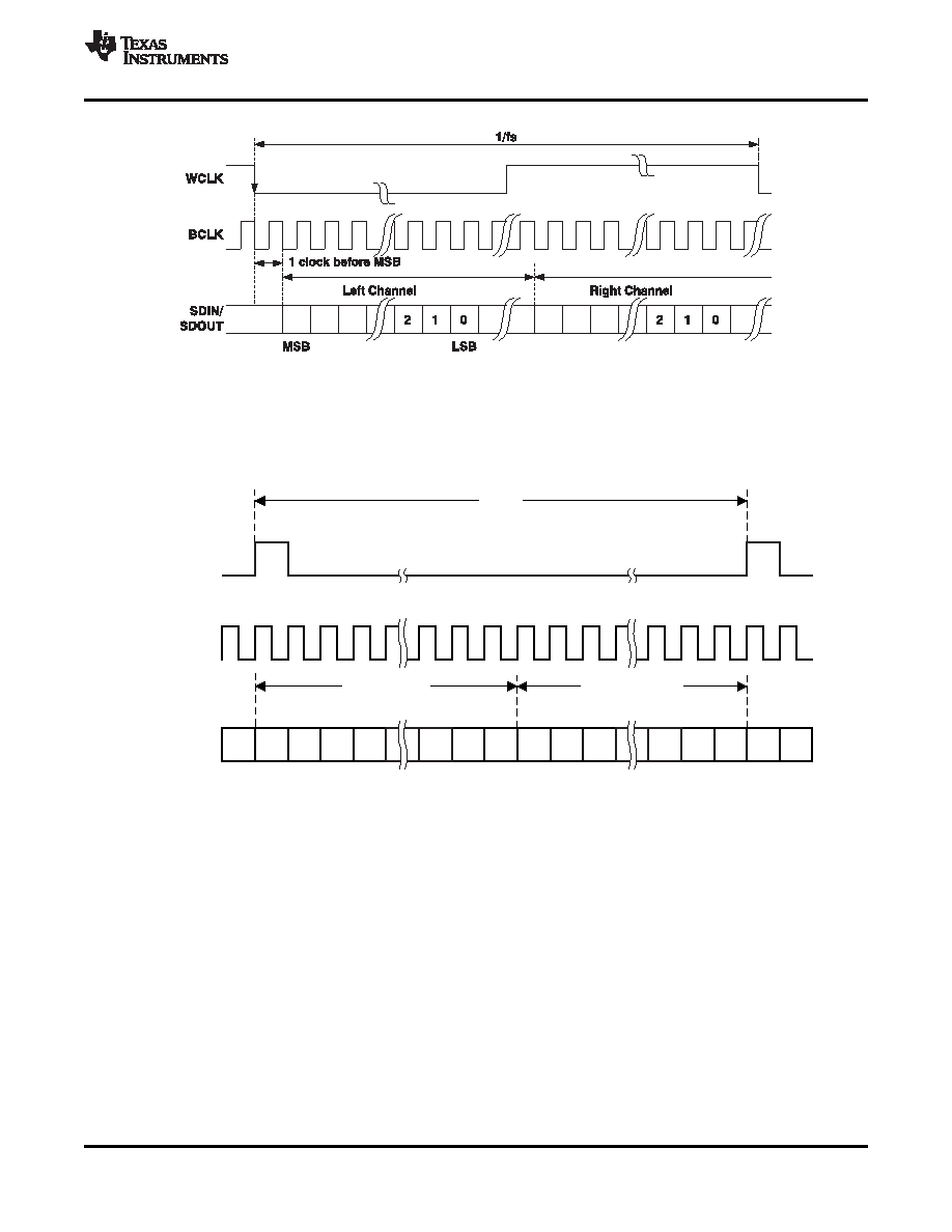
Figure 20. I2S Serial Data Bus Mode Operation
In DSP mode, the rising edge of the word clock starts the data transfer with the left channel data first and
immediately followed by the right channel data. Each data bit is valid on the falling edge of the bit clock.
Figure 21. DSP Serial Bus Mode Operation
Time-division multiplexed data transfer can be realized in any of the above transfer modes if the 256-clock bit
clock mode is selected, although it is recommended to be used in either left-justified mode or DSP mode. By
changing the programmable offset, the bit clock in each frame where the data begins can be changed, and the
serial data output driver (DOUT) can also be programmed to 3-state during all bit clocks except when valid data
is being put onto the bus. This allows other codecs to be programmed with different offsets and to drive their
data onto the same DOUT line, just in a different slot. For incoming data, the codec simply ignores data on the
bus except where it is expected based on the programmed offset.
Note that the location of the data when an offset is programmed is different, depending on what transfer mode is
selected. In DSP mode, both left and right channels of data are transferred immediately adjacent to each other in
the frame. This differs from left-justified mode, where the left and right channel data will always be a half-frame
apart in each frame. In this case, as the offset is programmed from zero to some higher value, both the left and
right channel data move across the frame, but still stay a full half-frame apart from each other. This is depicted in
Figure 22 for the two cases.
Copyright 2008–2009, Texas Instruments Incorporated
23
Product Folder Link(s): TLV320AIC3107
相关PDF资料 |
PDF描述 |
|---|---|
| TLV320AIC3107YZFR | 2 CHANNEL, AUDIO AMPLIFIER, PBGA42 |
| TLV320AIC3110IRHBR | AUDIO AMPLIFIER, PQCC32 |
| TLV320AIC3110IRHBT | AUDIO AMPLIFIER, PQCC32 |
| TLV320AIC3111IRHBT | AUDIO AMPLIFIER, PQCC32 |
| TLV320AIC3111IRHBR | AUDIO AMPLIFIER, PQCC32 |
相关代理商/技术参数 |
参数描述 |
|---|---|
| TLV320AIC3107IRSBT | 功能描述:接口—CODEC Low Pwr Stereo CODEC RoHS:否 制造商:Texas Instruments 类型: 分辨率: 转换速率:48 kSPs 接口类型:I2C ADC 数量:2 DAC 数量:4 工作电源电压:1.8 V, 2.1 V, 2.3 V to 5.5 V 最大工作温度:+ 85 C 安装风格:SMD/SMT 封装 / 箱体:DSBGA-81 封装:Reel |
| TLV320AIC3107IYZFR | 功能描述:接口—CODEC Low-Pwr Stereo CODEC RoHS:否 制造商:Texas Instruments 类型: 分辨率: 转换速率:48 kSPs 接口类型:I2C ADC 数量:2 DAC 数量:4 工作电源电压:1.8 V, 2.1 V, 2.3 V to 5.5 V 最大工作温度:+ 85 C 安装风格:SMD/SMT 封装 / 箱体:DSBGA-81 封装:Reel |
| TLV320AIC3107IYZFT | 功能描述:接口—CODEC Low-Pwr Stereo CODEC RoHS:否 制造商:Texas Instruments 类型: 分辨率: 转换速率:48 kSPs 接口类型:I2C ADC 数量:2 DAC 数量:4 工作电源电压:1.8 V, 2.1 V, 2.3 V to 5.5 V 最大工作温度:+ 85 C 安装风格:SMD/SMT 封装 / 箱体:DSBGA-81 封装:Reel |
| TLV320AIC3107YZFR | 制造商:TI 制造商全称:Texas Instruments 功能描述:LOW-POWER STEREO CODEC WITH INTEGRATED MONO CLASS-D SPEAKER AMPLIFIER |
| TLV320AIC3110 | 制造商:TI 制造商全称:Texas Instruments 功能描述:Low-Power Audio Codec With Audio Procsessing and Stereo Class-D Speaker Amplifier |
发布紧急采购,3分钟左右您将得到回复。