- 您现在的位置:买卖IC网 > PDF目录98253 > TLV320AIC3107IRSBT (TEXAS INSTRUMENTS INC) 2 CHANNEL, AUDIO AMPLIFIER, PQCC40 PDF资料下载
参数资料
| 型号: | TLV320AIC3107IRSBT |
| 厂商: | TEXAS INSTRUMENTS INC |
| 元件分类: | 音频/视频放大 |
| 英文描述: | 2 CHANNEL, AUDIO AMPLIFIER, PQCC40 |
| 封装: | 5 X 5 MM, 0.40 MM PITCH, GREEN, PLASTIC, WQFN-40 |
| 文件页数: | 14/99页 |
| 文件大小: | 1474K |
| 代理商: | TLV320AIC3107IRSBT |
第1页第2页第3页第4页第5页第6页第7页第8页第9页第10页第11页第12页第13页当前第14页第15页第16页第17页第18页第19页第20页第21页第22页第23页第24页第25页第26页第27页第28页第29页第30页第31页第32页第33页第34页第35页第36页第37页第38页第39页第40页第41页第42页第43页第44页第45页第46页第47页第48页第49页第50页第51页第52页第53页第54页第55页第56页第57页第58页第59页第60页第61页第62页第63页第64页第65页第66页第67页第68页第69页第70页第71页第72页第73页第74页第75页第76页第77页第78页第79页第80页第81页第82页第83页第84页第85页第86页第87页第88页第89页第90页第91页第92页第93页第94页第95页第96页第97页第98页第99页
DA(6)
DA(0)
RA(7)
RA(0)
Start
(M)
7-bit Device Address
(M)
Write
(M)
Slave
Ack
(S)
8-bit Register Address
(M)
Slave
Ack
(S)
SDA
SCL
DA(6)
DA(0)
7-bit Device Address
(M)
Read
(M)
Slave
Ack
(S)
D(7)
D(0)
8-bit Register Data
(S)
Stop
(M)
Master
No Ack
(M)
Repeat
Start
(M)
(M) => SDA Controlled by Master
(S) => SDA Controlled by Slave
I
2C BUS DEBUG IN A GLITCHED SYSTEM
DIGITAL AUDIO DATA SERIAL INTERFACE
www.ti.com .............................................................................................................................................. SLOS545C – NOVEMBER 2008 – REVISED MARCH 2009
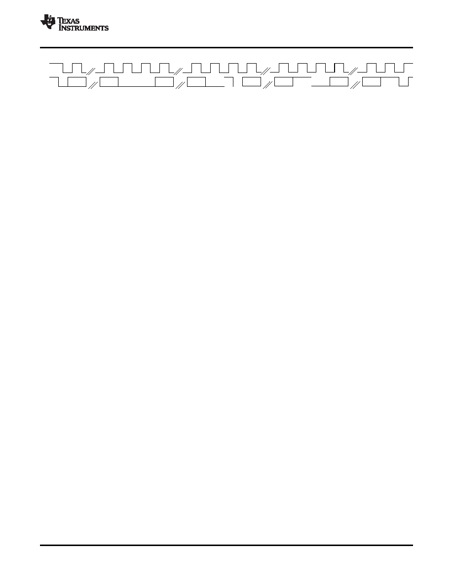
Figure 17. I2C Read
In the case of an I2C register write, if the master does not issue a STOP condition, then the device enters
auto-increment mode. So in the next eight clocks, the data on SDA is treated as data for the next incremental
register.
Similarly, in the case of an I2C register read, after the device has sent out the 8-bit data from the addressed
register, if the master issues an ACKNOWLEDGE, the slave takes over control of SDA bus and transmit for the
next 8 clocks the data of the next incremental register.
Occasionally, some systems may encounter noise or glitches on the I2C bus. In the unlikely event that this
affects bus performance, then it can be useful to use the I2C Debug register. This feature terminates the I2C bus
error allowing this I2C device and system to resume communications. The I2C bus error detector is enabled by
default. The TLV320AIC3107 I2C error detector status can be read from Page 0, Register 107, bit D0. If desired,
the detector can be disabled by writing to Page 0, Register 107, bit D2.
Audio data is transferred between the host processor and the TLV320AIC3107 via the digital audio data serial
interface, or audio bus. The audio bus on this device is flexible, including left or right justified data options,
support for I2S or PCM protocols, programmable data length options, a TDM mode for multichannel operation,
flexible master/slave configurability for each bus clock line, and the ability to communicate with multiple devices
within a system directly.
The audio bus of the TLV320AIC3107 can be configured for left or right justified, I2S, DSP, or TDM modes of
operation, where communication with standard telephony PCM interfaces is supported within the TDM mode.
These modes are all MSB-first, with data width programmable as 16, 20, 24, or 32 bits. In addition, the word
clock (WCLK or GPIO1) and bit clock (BCLK) can be independently configured in either Master or Slave mode,
for flexible connectivity to a wide variety of processors
The word clock (WCLK or GPIO1) is used to define the beginning of a frame, and may be programmed as either
a pulse or a square-wave signal. The frequency of this clock corresponds to the maximum of the selected ADC
and DAC sampling frequencies.
The bit clock (BCLK) is used to clock in and out the digital audio data across the serial bus. When in Master
mode, this signal can be programmed in two further modes: continuous transfer mode, and 256-clock mode. In
continuous transfer mode, only the minimal number of bit clocks needed to transfer the audio data are generated,
so in general the number of bit clocks per frame will be two times the data width. For example, if data width is
chosen as 16-bits, then 32 bit clocks will be generated per frame. If the bit clock signal in master mode will be
used by a PLL in another device, it is recommended that the 16-bit or 32-bit data width selections be used.
These cases result in a low jitter bit clock signal being generated, having frequencies of 32×Fs or 64×Fs. In the
cases of 20-bit and 24-bit data width in master mode, the bit clocks generated in each frame will not all be of
equal period, due to the device not having a clean 40×Fs or 48×Fs clock signal readily available. The average
frequency of the bit clock signal is still accurate in these cases (being 40×Fs or 48×Fs), but the resulting clock
signal has higher jitter than in the 16-bit and 32-bit cases.
In 256-clock mode, a constant 256 bit clocks per frame are generated, independent of the data width chosen.
The TLV320AIC3107 further includes programmability to 3-state the DOUT line during all bit clocks when valid
data is not being sent. By combining this capability with the ability to program at what bit clock in a frame the
audio data will begin, time-division multiplexing (TDM) can be accomplished, resulting in multiple codecs able to
use a single audio serial data bus.
Copyright 2008–2009, Texas Instruments Incorporated
21
Product Folder Link(s): TLV320AIC3107
相关PDF资料 |
PDF描述 |
|---|---|
| TLV320AIC3107IRSBR | 2 CHANNEL, AUDIO AMPLIFIER, PQCC40 |
| TLV320AIC3107YZFR | 2 CHANNEL, AUDIO AMPLIFIER, PBGA42 |
| TLV320AIC3110IRHBR | AUDIO AMPLIFIER, PQCC32 |
| TLV320AIC3110IRHBT | AUDIO AMPLIFIER, PQCC32 |
| TLV320AIC3111IRHBT | AUDIO AMPLIFIER, PQCC32 |
相关代理商/技术参数 |
参数描述 |
|---|---|
| TLV320AIC3107IYZFR | 功能描述:接口—CODEC Low-Pwr Stereo CODEC RoHS:否 制造商:Texas Instruments 类型: 分辨率: 转换速率:48 kSPs 接口类型:I2C ADC 数量:2 DAC 数量:4 工作电源电压:1.8 V, 2.1 V, 2.3 V to 5.5 V 最大工作温度:+ 85 C 安装风格:SMD/SMT 封装 / 箱体:DSBGA-81 封装:Reel |
| TLV320AIC3107IYZFT | 功能描述:接口—CODEC Low-Pwr Stereo CODEC RoHS:否 制造商:Texas Instruments 类型: 分辨率: 转换速率:48 kSPs 接口类型:I2C ADC 数量:2 DAC 数量:4 工作电源电压:1.8 V, 2.1 V, 2.3 V to 5.5 V 最大工作温度:+ 85 C 安装风格:SMD/SMT 封装 / 箱体:DSBGA-81 封装:Reel |
| TLV320AIC3107YZFR | 制造商:TI 制造商全称:Texas Instruments 功能描述:LOW-POWER STEREO CODEC WITH INTEGRATED MONO CLASS-D SPEAKER AMPLIFIER |
| TLV320AIC3110 | 制造商:TI 制造商全称:Texas Instruments 功能描述:Low-Power Audio Codec With Audio Procsessing and Stereo Class-D Speaker Amplifier |
| TLV320AIC3110EVM-U | 功能描述:音频 IC 开发工具 TLV320AIC3110EVM-U Eval Mod RoHS:否 制造商:Texas Instruments 产品:Evaluation Kits 类型:Audio Amplifiers 工具用于评估:TAS5614L 工作电源电压:12 V to 38 V |
发布紧急采购,3分钟左右您将得到回复。