- 您现在的位置:买卖IC网 > PDF目录98255 > TLV5580IPWRG4 (TEXAS INSTRUMENTS INC) 1-CH 8-BIT PROPRIETARY METHOD ADC, PARALLEL ACCESS, PDSO28 PDF资料下载
参数资料
| 型号: | TLV5580IPWRG4 |
| 厂商: | TEXAS INSTRUMENTS INC |
| 元件分类: | ADC |
| 英文描述: | 1-CH 8-BIT PROPRIETARY METHOD ADC, PARALLEL ACCESS, PDSO28 |
| 封装: | GREEN, PLASTIC, TSSOP-28 |
| 文件页数: | 31/36页 |
| 文件大小: | 478K |
| 代理商: | TLV5580IPWRG4 |
第1页第2页第3页第4页第5页第6页第7页第8页第9页第10页第11页第12页第13页第14页第15页第16页第17页第18页第19页第20页第21页第22页第23页第24页第25页第26页第27页第28页第29页第30页当前第31页第32页第33页第34页第35页第36页
TLV5580
8BIT, 80 MSPS LOW POWER A/D CONVERTER
SLAS205B DECEMBER 1998 REVISED OCTOBER 2003
www.ti.com
4
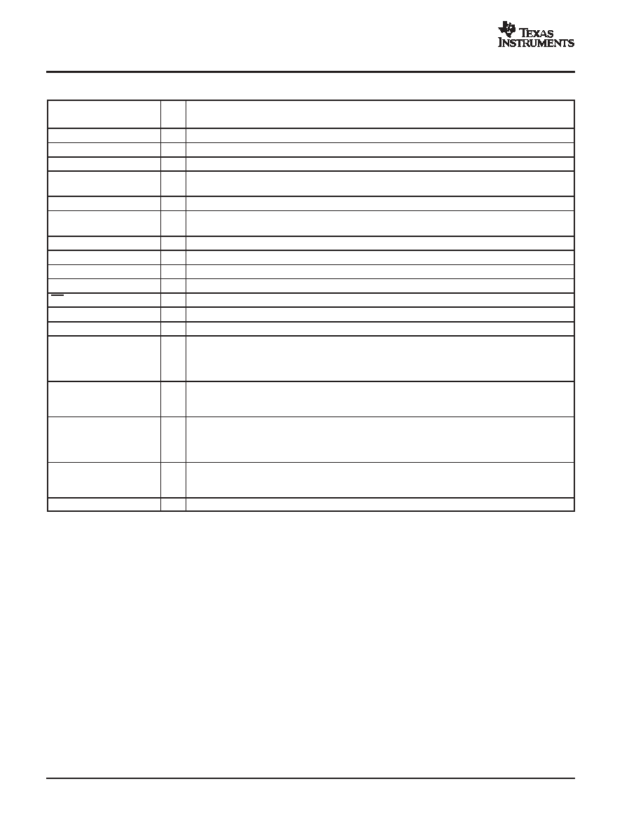
Terminal Functions
TERMINAL
I/O
DESCRIPTION
NAME
NO.
I/O
DESCRIPTION
AIN
26
I
Analog input
AVDD
16, 27
I
Analog supply voltage
AVSS
18, 23, 28
I
Analog ground
BG
17
O
Band gap reference voltage. A 1
F capacitor (with an optional 0.1 F capacitor in parallel) should be
connected between this terminal and AVSS for external filtering.
CLK
12
I
Clock input. The input is sampled on each rising edge of CLK.
CML
25
O
Common mode level. This voltage is equal to (AVDD AVSS) ÷ 2. An external 0.1 F capacitor should be
connected between this terminal and AVSS.
D0 D7
2 9
O
Data outputs. D7 is the MSB
DRVDD
1
I
Supply voltage for digital output drivers
DRVSS
10
I
Ground for digital output drivers
DVDD
14
I
Digital supply voltage
OE
13
I
Output enable. When high the D0 D7 outputs go in high-impedance mode.
DVSS
11
I
Digital ground
PWDN_REF
24
I
Power down for internal reference voltages. A high on this terminal will disable the internal reference circuit.
REFBI
21
I
Reference voltage bottom input. The voltage at this terminal defines the bottom reference voltage for the
ADC. It can be connected to REFBO or to an externally generated reference level. Sufficient filtering should
be applied to this input. The use a 0.1
F capacitor connected between REFBI and AVSS is recommended.
Additionally, a 0.1
F capacitor can be connected between REFTI and REFBI.
REFBO
22
O
Reference voltage bottom output. An internally generated reference is available at this terminal. It can be
connected to REFBI or left unconnected. A 1
F capacitor between REFBO and AVSS will provide sufficient
decoupling required for this output.
REFTI
20
I
Reference voltage top input. The voltage at this terminal defines the top reference voltage for the ADC. It
can be connected to REFTO or to an externally generated reference level. Sufficient filtering should be
applied to this input. The use of a 0.1
F capacitor between REFTI and AVSS is recommended. Additionally,
a 0.1
F capacitor can be connected between REFTI and REFBI.
REFTO
19
O
Reference voltage top output. An internally generated reference is available at this terminal. It can be
connected to REFTI or left unconnected. A 1
F capacitor between REFTO and AVSS will provide sufficient
decoupling required for this output.
STBY
15
I
Standby input. A high level on this input enables a power-down mode.
相关PDF资料 |
PDF描述 |
|---|---|
| TLV5580IDWR | 1-CH 8-BIT PROPRIETARY METHOD ADC, PARALLEL ACCESS, PDSO28 |
| TLV5580IPW | 1-CH 8-BIT PROPRIETARY METHOD ADC, PARALLEL ACCESS, PDSO28 |
| TLV5580IPWR | 1-CH 8-BIT PROPRIETARY METHOD ADC, PARALLEL ACCESS, PDSO28 |
| TLV5580IDWG4 | 1-CH 8-BIT PROPRIETARY METHOD ADC, PARALLEL ACCESS, PDSO28 |
| TLV5580CDWG4 | 1-CH 8-BIT PROPRIETARY METHOD ADC, PARALLEL ACCESS, PDSO28 |
相关代理商/技术参数 |
参数描述 |
|---|---|
| TLV5580PW | 制造商:TI 制造商全称:Texas Instruments 功能描述:8-BIT, 80 MSPS LOW-POWER A/D CONVERTER |
| TLV5590 | 制造商:TI 制造商全称:Texas Instruments 功能描述:2-BIT ANALOG-TO-DIGITAL CONVERTER FOR FLEX |
| TLV5590ED | 制造商:Rochester Electronics LLC 功能描述:- Bulk |
| TLV5590EDR | 制造商:Rochester Electronics LLC 功能描述:- Bulk |
| TLV5590EPWR | 制造商:Texas Instruments 功能描述: |
发布紧急采购,3分钟左右您将得到回复。