- 您现在的位置:买卖IC网 > PDF目录67343 > TLV5618AQD (TEXAS INSTRUMENTS INC) SERIAL INPUT LOADING, 3 us SETTLING TIME, 12-BIT DAC, PDSO8 PDF资料下载
参数资料
| 型号: | TLV5618AQD |
| 厂商: | TEXAS INSTRUMENTS INC |
| 元件分类: | DAC |
| 英文描述: | SERIAL INPUT LOADING, 3 us SETTLING TIME, 12-BIT DAC, PDSO8 |
| 封装: | PLASTIC, SOIC-8 |
| 文件页数: | 2/23页 |
| 文件大小: | 633K |
| 代理商: | TLV5618AQD |
TLV5618A
2.7-V TO 5.5-V LOW-POWER DUAL 12-BIT
DIGITAL-TO-ANALOG CONVERTER WITH POWER DOWN
SLAS230H – JULY 1999 – REVISED JULY 2002
10
POST OFFICE BOX 655303
DALLAS, TEXAS 75265
APPLICATION INFORMATION
general function
The TLV5618A is a dual 12-bit, single-supply DAC, based on a resistor-string architecture. It consists of a serial
interface, a speed and power down control logic, a resistor string, and a rail-to-rail output buffer.
The output voltage (full scale determined by the reference) is given by:
2REF
CODE
2n
[V]
Where REF is the reference voltage and CODE is the digital input value within the range of 010 to 2n–1, where
n=12 (bits). The 16-bit data word, consisting of control bits and the new DAC value, is illustrated in the data
format section. A power-on reset initially resets the internal latches to a defined state (all bits zero).
serial interface
A falling edge of CS starts shifting the data bit-per-bit (starting with the MSB) to the internal register on the falling
edges of SCLK. After 16 bits have been transferred or CS rises, the content of the shift register is moved to the
target latches (DAC A, DAC B, BUFFER, CONTROL), depending on the control bits within the data word.
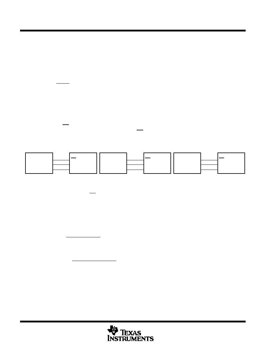
Figure 12 shows examples of how to connect the TLV5618A to TMS320, SPI, and Microwire.
TMS320
DSP FSX
CLKX
DX
TLV5618A
SCLK
DIN
CS
SPI
I/O
SCK
MOSI
TLV5618A
SCLK
DIN
CS
Microwire
I/O
SK
SO
TLV5618A
SCLK
DIN
CS
Figure 12. Three-Wire Interface
Notes on SPI and Microwire: Before the controller starts the data transfer, the software has to generate a falling
edge on the pin connected to CS. If the word width is 8 bits (SPI and Microwire) two write operations must be
performed to program the TLV5618A. After the write operation(s), the holding registers or the control register
are updated automatically on the next positive clock edge following the 16th falling clock edge.
serial clock frequency and update rate
The maximum serial clock frequency is given by:
f
sclkmax +
1
t
whmin )
t
wlmin
+ 20 MHz
The maximum update rate is:
f
updatemax +
1
16 t
whmin )
t
wlmin
+ 1.25 MHz
Note that the maximum update rate is just a theoretical value for the serial interface, as the settling time of the
TLV5618A should also be considered.
相关PDF资料 |
PDF描述 |
|---|---|
| TLV5618AMFKB | SERIAL INPUT LOADING, 3 us SETTLING TIME, 12-BIT DAC, CQCC20 |
| TLV5618ACD | SERIAL INPUT LOADING, 3 us SETTLING TIME, 12-BIT DAC, PDSO8 |
| TLV5618AIDG4 | SERIAL INPUT LOADING, 3 us SETTLING TIME, 12-BIT DAC, PDSO8 |
| TLV5618AMFK | SERIAL INPUT LOADING, 3 us SETTLING TIME, 12-BIT DAC, CQCC20 |
| 5962-9955702Q2A | SERIAL INPUT LOADING, 12.5 us SETTLING TIME, 12-BIT DAC, CQCC20 |
相关代理商/技术参数 |
参数描述 |
|---|---|
| TLV5618AQDG4 | 功能描述:数模转换器- DAC 12B 2.5 us Dual DAC RoHS:否 制造商:Texas Instruments 转换器数量:1 DAC 输出端数量:1 转换速率:2 MSPs 分辨率:16 bit 接口类型:QSPI, SPI, Serial (3-Wire, Microwire) 稳定时间:1 us 最大工作温度:+ 85 C 安装风格:SMD/SMT 封装 / 箱体:SOIC-14 封装:Tube |
| TLV5618AQDR | 功能描述:数模转换器- DAC 12 Bit 2.5 us Dual DAC Serial Input RoHS:否 制造商:Texas Instruments 转换器数量:1 DAC 输出端数量:1 转换速率:2 MSPs 分辨率:16 bit 接口类型:QSPI, SPI, Serial (3-Wire, Microwire) 稳定时间:1 us 最大工作温度:+ 85 C 安装风格:SMD/SMT 封装 / 箱体:SOIC-14 封装:Tube |
| TLV5618AQDRG4 | 功能描述:数模转换器- DAC 12B 2.5 us Dual DAC RoHS:否 制造商:Texas Instruments 转换器数量:1 DAC 输出端数量:1 转换速率:2 MSPs 分辨率:16 bit 接口类型:QSPI, SPI, Serial (3-Wire, Microwire) 稳定时间:1 us 最大工作温度:+ 85 C 安装风格:SMD/SMT 封装 / 箱体:SOIC-14 封装:Tube |
| TLV5619 | 制造商:TI 制造商全称:Texas Instruments 功能描述:2.7 V TO 5.5 V 12-BIT PARALLEL DIGITAL-TO-ANALOG CONVERTER WITH POWER DOWN |
| TLV5619CDW | 功能描述:数模转换器- DAC 12bit CMOS DAC RoHS:否 制造商:Texas Instruments 转换器数量:1 DAC 输出端数量:1 转换速率:2 MSPs 分辨率:16 bit 接口类型:QSPI, SPI, Serial (3-Wire, Microwire) 稳定时间:1 us 最大工作温度:+ 85 C 安装风格:SMD/SMT 封装 / 箱体:SOIC-14 封装:Tube |
发布紧急采购,3分钟左右您将得到回复。