- 您现在的位置:买卖IC网 > PDF目录98262 > TLV571IPWR (TEXAS INSTRUMENTS INC) 1-CH 8-BIT SUCCESSIVE APPROXIMATION ADC, PARALLEL ACCESS, PDSO24 PDF资料下载
参数资料
| 型号: | TLV571IPWR |
| 厂商: | TEXAS INSTRUMENTS INC |
| 元件分类: | ADC |
| 英文描述: | 1-CH 8-BIT SUCCESSIVE APPROXIMATION ADC, PARALLEL ACCESS, PDSO24 |
| 封装: | GREEN, PLASTIC, TSSOP-24 |
| 文件页数: | 6/28页 |
| 文件大小: | 479K |
| 代理商: | TLV571IPWR |
第1页第2页第3页第4页第5页当前第6页第7页第8页第9页第10页第11页第12页第13页第14页第15页第16页第17页第18页第19页第20页第21页第22页第23页第24页第25页第26页第27页第28页
TLV571
2.7 V TO 5.5 V, 1-CHANNEL, 8-BIT,
PARALLEL ANALOG-TO-DIGITAL CONVERTER
SLAS239A – SEPTEMBER 1999 – REVISED FEBRUARY 2000
14
POST OFFICE BOX 655303
DALLAS, TEXAS 75265
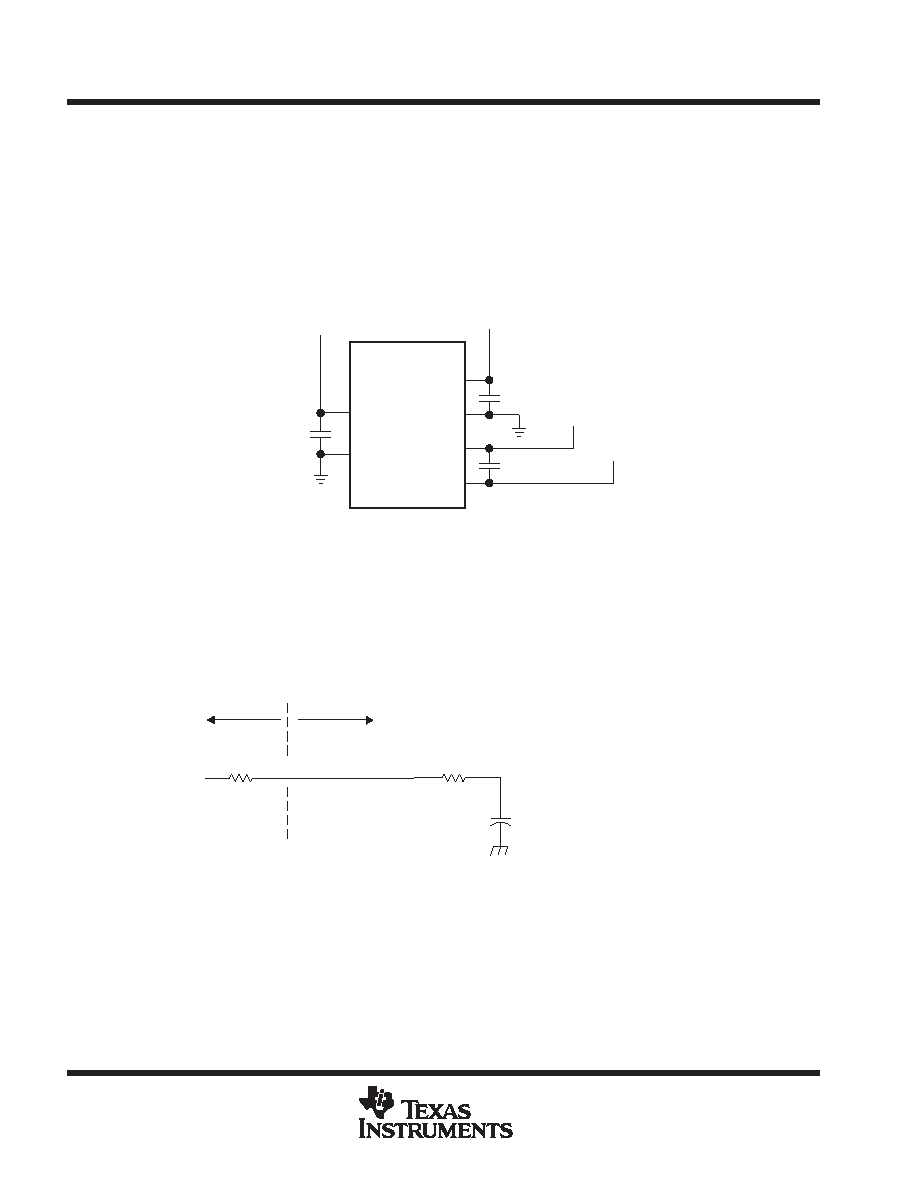
grounding and decoupling considerations
General practices should apply to the PCB design to limit high frequency transients and noise that are fed back
into the supply and reference lines. This requires that the supply and reference pins be sufficiently bypassed.
In most cases 0.1-
F ceramic chip capacitors are adequate to keep the impedance low over a wide frequency
range. Since their effectiveness depends largely on the proximity to the individual supply pin, they should be
placed as close to the supply pins as possible.
To reduce high frequency and noise coupling, it is highly recommended that digital and analog grounds be
shorted immediately outside the package. This can be accomplished by running a low impedance line between
DGND and AGND under the package.
TLV571
100 nF
DGND
DVDD
AVDD
AGND
REFP
REFM
100 nF
VREFP
VREFM
AVDD
DVDD
Figure 9. Placement for Decoupling Capacitors
power supply ground layout
Printed-circuit boards that use separate analog and digital ground planes offer the best system performance.
Wire-wrap boards do not perform well and should not be used. The two ground planes should be connected
together at the low-impedance power-supply source. The best ground connection may be achieved by
connecting the ADC AGND terminal to the system analog ground plane making sure that analog ground
currents are well managed.
Rs
VS
VC
15 pF
Driving Source
TLV571
Ci
VI
VI = Input Voltage at AIN
VS = External Driving Source Voltage
Rs = Source Resistance
Ri(ADC)= Input Resistance of ADC
Ci = Input Capacitance
VC= Capacitance Charging Voltage
Driving source requirements:
Noise and distortion for the source must be equivalent to the resolution of the converter.
Rs must be real at the input frequency.
Ri(ADC)
AIN
Figure 10. Equivalent Input Circuit Including the Driving Source
相关PDF资料 |
PDF描述 |
|---|---|
| TLV571IDWG4 | 1-CH 8-BIT SUCCESSIVE APPROXIMATION ADC, PARALLEL ACCESS, PDSO24 |
| TLV571IDW | 1-CH 8-BIT SUCCESSIVE APPROXIMATION ADC, PARALLEL ACCESS, PDSO24 |
| TLV571IPWG4 | 1-CH 8-BIT SUCCESSIVE APPROXIMATION ADC, PARALLEL ACCESS, PDSO24 |
| TLV571IPW | 1-CH 8-BIT SUCCESSIVE APPROXIMATION ADC, PARALLEL ACCESS, PDSO24 |
| TLV5734PAG | 3-CH 8-BIT PROPRIETARY METHOD ADC, PARALLEL ACCESS, PQFP64 |
相关代理商/技术参数 |
参数描述 |
|---|---|
| TLV571PW | 制造商:TI 制造商全称:Texas Instruments 功能描述:2.7 V TO 5.5 V, 1-CHANNEL, 8-BIT, PARALLEL ANALOG-TO-DIGITAL CONVERTER |
| TLV5734 | 制造商:TI 制造商全称:Texas Instruments 功能描述:TRIPLE 8 BIT 30 MSPS ADC WITH HIGH -PRECISION CLAMP FOR YUV/RGB VIDEO |
| TLV5734PAG | 功能描述:视频模拟/数字化转换器集成电路 8B 30MSPS ADC Triple Ch Digital Clamp RoHS:否 制造商:Texas Instruments 输入信号类型:Differential 转换器数量:1 ADC 输入端数量:4 转换速率:3 Gbps 分辨率:8 bit 结构: 输入电压:3.3 V 接口类型:SPI 信噪比: 电压参考: 电源电压-最大:3.45 V 电源电压-最小:3.15 V 最大功率耗散: 最大工作温度:+ 85 C 最小工作温度:- 40 C 封装 / 箱体:TCSP-48 封装:Reel |
| TLV5734PAGG4 | 功能描述:视频模拟/数字化转换器集成电路 8B 30 MSPS ADC 3Ch RoHS:否 制造商:Texas Instruments 输入信号类型:Differential 转换器数量:1 ADC 输入端数量:4 转换速率:3 Gbps 分辨率:8 bit 结构: 输入电压:3.3 V 接口类型:SPI 信噪比: 电压参考: 电源电压-最大:3.45 V 电源电压-最小:3.15 V 最大功率耗散: 最大工作温度:+ 85 C 最小工作温度:- 40 C 封装 / 箱体:TCSP-48 封装:Reel |
| TLV6001IDBVR | 功能描述:IC OP AMP RR 1MHZ SOT23-5 制造商:texas instruments 系列:- 包装:剪切带(CT) 零件状态:在售 放大器类型:通用 电路数:1 输出类型:满摆幅 压摆率:0.5 V/μs 增益带宽积:1MHz 电流 - 输入偏置:1pA 电压 - 输入失调:750μV 电流 - 电源:75μA 电压 - 电源,单/双(±):1.8 V ~ 5.5 V,±0.9 V ~ 2.75 V 工作温度:-40°C ~ 125°C 安装类型:表面贴装 封装/外壳:SC-74A,SOT-753 供应商器件封装:SOT-23-5 标准包装:1 |
发布紧急采购,3分钟左右您将得到回复。